With its suitability for monolithic integration for optics and photonics, silicon has been widely hailed as the material of the future. But graphene — with its capacity for signal emission, transmission and detection — could be the next disruptive technology.
Last July, the U.S. unveiled a national institute for integrated photonics backed by $600 million in federal, state and private funding. The Rochester, N.Y.-based American Institute for Manufacturing Integrated Photonics, better known as AIM Photonics, brings together academia, federal research institutions and companies in an effort to emulate the successes of the electronics industry over the past 40 years.
The reason for the fanfare and concerted effort lies in the exciting breakthroughs integrated photonics promises: the development of chips capable of controlling the relative phase of light for use in robotics or self-driving cars; biological and chemical sensors that can detect even the subtlest environmental change; optical computing; and data communications.
Indeed, integrated photonics — a term that encompasses the design and fabrication of electronic/photonic devices and their components on a chip — is on the precipice of exciting breakthroughs.
“These electronic-photonic chips will represent a new paradigm in circuit design and enable a wide range of future applications including: high bandwidth, low power interconnects within chips and between them; highly sensitive biological/chemical sensors that exploit the interference properties of light; and analog photonic chips for RF signal transmission and processing in cellular networks and radar,” said Stefan Preble, Ph.D., director of Rochester Institute of Technology’s (RIT) Integrated Photonics Group, who is leading the integrated photonics efforts of RIT’s Future Photon Initiative.
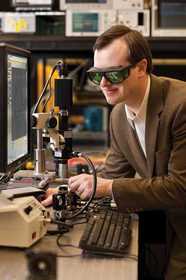
Stefan Preble, director of Rochester Institute of Technology’s Integrated Photonics Group, at work in his lab. Courtesy of John Myers/Myers Creative Imaging.
Today’s integrated photonic circuits are rudimentary compared to the complexity of today’s electronic circuits. Yet they are likely to be far more complex — by orders of magnitude — within five to 10 years, as the technology matures and electronic and photonic functionalities are integrated, Preble said.
He, like others, draws strong parallels with where photonics technologies are today and where microelectronics were 40 years ago.
“In the ’70s, there were only thousands of transistors in computer chips, but because of improvements in integrated circuit manufacturing, it is now possible to have billions of transistors in the same footprint,” Preble said. “It’s well-known that the density of these circuits has traditionally followed Moore’s law, where the number of transistors on a given wafer doubles every two years.”
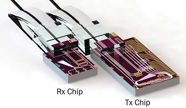
A silicon photonics 100Gb/s and 200Gb/s wave division multiplexing (WDM) chipset. Courtesy of Mellanox Technologies.
Potential of silicon ‘enormous’
For that trajectory to occur, researchers must continue to push the boundaries when it comes to materials.
The first advances came in the late ’90s with the development of planar
waveguides that were created out of glass substrates using
photolithography. Efforts to insert these waveguides into integrated
circuits were soon abandoned as they proved to be too large for use on
circuits, and problems arose integrating both lasers and detectors, due
to incongruities with the materials.
By the early 2000s, all eyes were on silicon, with its high refractive index and capabilities that included confining light and support for internal reflection. It’s also transparent in the same wavelength regions used in fiber optics (1300 to 1600 nm).
But along with these characteristics came another: silicon’s compatibility with traditional CMOS manufacturing. Done in volume, CMOS manufacturing can be very inexpensive and makes use of the same infrastructure in place for manufacturing microelectronics.
“Silicon waveguides have inherent cost advantages over other integrated photonic technologies,” Preble said. “Furthermore, silicon waveguides have proven to be more compact and operate with lower loss than III-V based waveguide platforms.”
One challenge is the difficulty — and cost — associated with packaging. Silicon photonic chips must be connected to optical fibers, and these fibers are significantly larger than the waveguides. This results in a large mismatch in energy confinement between the optical fiber
and nanophotonic waveguide, presenting a challenge in coupling light between the two.
Mode converters have been used to ease this transition, achieving coupling efficiency rates that exceed 70 percent. But these high efficiencies are only realized when the optical fibers are “actively” and precisely aligned. A laser and detector must be used to monitor the amount of light getting in and out of the chip, and then the fiber is locked in place using epoxy.
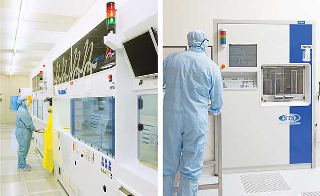
A high-volume production facility in Livingston, Scotland, is used to produce silica-on-silicon integrated optics and silicon MEMS wafers (above and right). Courtesy of Kaiam Corp.
“In order to solve the packaging issue, passive alignment techniques, similar to the pick-and-place tools commonly used for electronic chips, are required to overcome the time-sensitive active alignment being used today,” Preble said.
IBM, based in Armonk, N.Y., has been at the forefront of efforts in passive alignment.
Engineers there have been working on novel optical input/output (I/O) solutions aimed at low-cost, wide optical bandwidth and a large optical port count. Their approach involves leveraging fully automated microelectronic packaging facilities for photonic packaging specifically, and utilizing microelectronics wafer production facilities for photonic wafer fabrication. This is in contrast to today’s highly specialized, state-of-the art facilities with only partial automation.
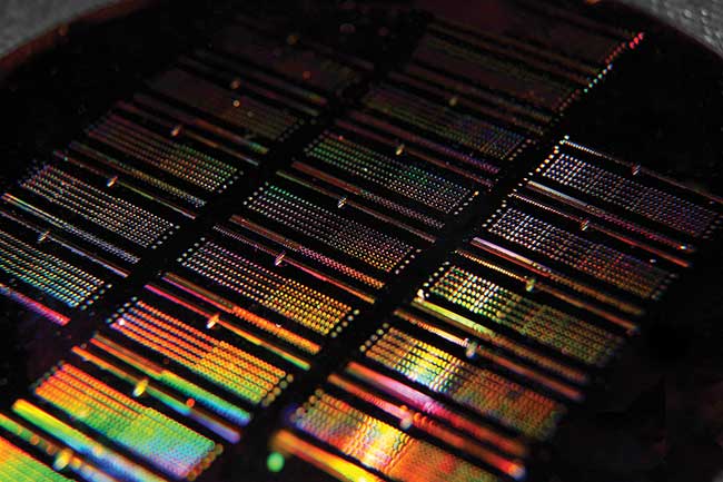
This working integrated photonic wafer created by Rochester Institute of Technology researchers contains thousands of integrated photonic devices including waveguides, filters, couplers, modulators and more. These integrated photonic chips will lead to higher performance sensors, computers and communication networks.
Another drawback for silicon is the difficulty in integrating lasers. Since silicon cannot be used as a laser material, traditional III-Vs such as gallium arsenide (GaAs) must be integrated on the same silicon wafer. And this must be done cost-effectively.
The first significant breakthrough came in 2006, when a team of researchers that included Intel’s Mario Paniccia and John Bowers of the University of California, Santa Barbara, discovered how to embed an electrically pumped AlGaInAs-silicon evanescent laser architecture in which the laser cavity was formed from silicon1.
More recently, new techniques have been developed for directly growing III-V lasers on silicon wafers. In 2014, another group led by John Bowers used a technique called beam epitaxy to grow quantum dot lasers on silicon.2

Integrated photonics will enable secure communication systems that exploit the quantum properties of light. Courtesy of Stefan Preble, Rochester Institute of Technology.
This March researchers from the University College London, University of Sheffield and Cardiff University unveiled a silicon-based laser that could be fully integrated on photonic and electronic circuits — without wafer bonding. The 1300-nm wavelength laser could operate at temperatures up to 120 °C for up to 100,000 hours.
“Realizing electrically pumped lasers based on [silicon] substrates is a fundamental step towards silicon photonics,” said Cardiff University professor Peter Smowton.
Conventional fabrication methods
Replicating these critical advances from the lab to a real-world manufacturing environment remains a work in progress.
An exciting development came last December, when researchers from the University of California, Berkeley, the Massachusetts Institute of Technology (MIT) and the University of Colorado, Boulder, used conventional fabrication methods in a foundry that mass produces computer chips to build what they said was the first fully integrated photonic chip that incorporated all the photonic interconnects (I/O) needed to communicate with other chips.3 The device consisted of two processor cores with more than 70 million transistors and 850 photonic components, and demonstrated a bandwidth density of 300 Gb/s per square millimeter, about 10 to 50 times greater than packaged electrical-only microprocessors on the market.
Today, a growing number of firms, including Intel, IBM and Cisco, are actively developing and commercializing silicon photonic technology. Mellanox Technologies, with headquarters in Sunnyvale, Calif., and Yokneam, Israel, is another of these pioneers, fabricating its own integrated circuits and switches for servers used in enterprise data centers.
The company’s silicon platforms are notable for efficiently supporting wavelength division multiplexing (WDM), which converts parallel channels into a single optical channel such as a waveguide or fiber strand. This optical integration reduces the fiber interconnect by a factor of eight, according to Arlon Martin, Mellanox’s senior director of marketing.
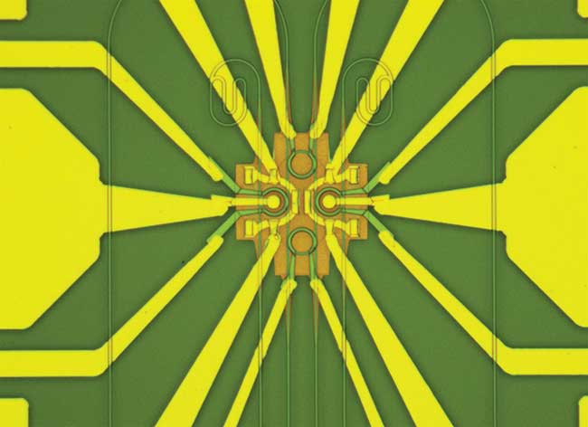
An on-chip circuit converts electrical data into photons. This combination allows information to be transferred at much higher rates with lower power. Courtesy of Stefan Preble, Rochester Institute of Technology.
Mellanox’s 200 Gb/s InfiniBand and Ethernet transceivers conform to the compact quad small form-factor pluggable (QSFP) — the most widely used package in data center connectivity. The enabling technologies are 50 Gb/s modulators and detectors built on silicon photonics.
“For silicon photonics, low-speed and low-cost lasers can be used, because the difficult, high-speed modulation is done in silicon,” Martin said.
Mellanox also achieved what it touts as an industry first: packaging lasers with direct coupling to the silicon chip — without a lens, isolator or filter. This eliminates the need for a transmitter optical subassembly (TOSA), which is an expensive step in that it requires optical alignment of multiple components. Alignment of the components within the TOSA must take place in a cleanroom environment, because even a tiny speck of dust would disrupt the laser.
Martin added: “In five to 10 years we will have Tb/s links using silicon photonics. We may see SiP integrated with switches, routers and servers/adapters for data center interconnects.”
Increasing demand for bandwidth
The ever-expanding appetite for bandwidth in the data center and beyond has led Newark, Calif.-based Kaiam to push the bounds of silicon photonic integration too.
The startup demonstrated a 100 Gigabit/s course wavelength division multiplexing silicon photonics transceiver, the CWDM4, at OFC 2016 in Mrch. The module combines all the high-speed electronics components together with high-performance silicon modulators and detectors in a single 3D stack. The silicon chip carries out transmit and received functions via silicon modulators and silicon receivers.
“Kaiam’s ability to easily and accurately assemble the silicon photonics chip in the module, as well as couple light on and off the chip efficiently, has made the technology feasible from a transceiver perspective, at this early stage, with room for more silicon advancements that [will] pave the way for a fully integrated photonics chip,” said Ramsey Selim, senior design engineer for Kaiam.
The next step will be getting light from the silicon chip to the fiber directly, which is a technical challenge for the moment, he said.
Selim echoed the advantages of silicon as the material of choice, given the huge investments in the semiconductor infrastructure, while the small feature size of silicon chips — and subsequent smaller footprint — enables lower-cost, high-volume manufacturing.
“Permanently tuning the waveguide properties post fabrication is still a challenge,” Selim said. “The technology is still limited by the lack of a silicon laser, although some companies are bonding III-V lasers directly onto the silicon chips.”
Graphene: 2D material of the future
If silicon is the material of today — and the foreseeable future — then graphene represents the next frontier.
In its simplest terms, graphene is a thin layer of pure carbon atoms that are bonded together in a hexagonal honeycomb lattice. Not only is it the thinnest crystal structure known at one atom thick, but also the strongest compound discovered — several hundred times stronger than steel, as well as being the best conductor of heat at room temperature and also the best known conductor of electricity.
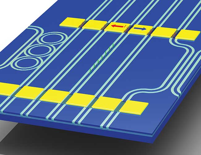
Graphene and other two-dimensional materials are being developed as active components on photonic integrated circuits. In this image, photonic modulators (bottom row) encode data in digital pulses carved from a continuous-wave input laser. These pulses are detected by chip-integrated photodetectors (top row). Other optical components such as ring filters and beamsplitters can be integrated on the same circuit. Courtesy of R.J. Shiue and D. Englund.
Graphene is capable of strong light-matter interactions, and high optical nonlinearity, allowing for all-optical signal processing. This avoids the need for the conversion of the optical signal to the electrical, bypassing the need to design high-speed interfaces between optical electronic parts.
“Graphene alone assembles a multiplicity of functions such as signal emission, transmission, modulation and detection,” said Eva Campo, Ph.D., a professor at the School of Electronic Engineering at Bangor University in Wales. “In comparison with silicon and even III-Vs, graphene’s properties are superior in terms of thermal conductivity, optical damage threshold and also third-order optical nonlinearities.”

Eva Campo and her research team in the lab at Bangor University in the U.K. Courtesy of Matter Dynamics Lab.
These properties make it ideal for optical communications — specifically photodetectors in the mid-infrared and long-wave range, nonlinear optics and mode-locked lasers, said Dirk Englund, an assistant professor of electrical engineering and computer science at MIT in Cambridge, Mass.
“In optical communications, you need a way of encoding signals on the transmitter side and detecting them on the receiver side. If this light is in the telecom band — about 1.5 µm in wavelength — then it can transmit through silicon with low attenuation,” he said.
As a result, it’s possible to guide telecom light in silicon waveguides in a photonic circuit.
To encode information onto the intensity of the light, a modulator is needed. That’s where graphene, with its strong tunability, has shown promise
.
“Since the telecom laser is below the bandgap of silicon [and] not absorbed, silicon itself doesn’t make a good detector. Graphene can again help here since it allows very fast photodetection,” Englund said.
Future promise
Still, there are considerable hurdles impeding commercialization. At the SPIE Photonics Europe Conference in Brussels in April, experts noted that graphene wasn’t yet at a point suitable for front-end integration on integrated circuits, where Campo said graphene can really outperform current technologies. The issues cited at the SPIE forum included CMOS scalability and material performance — both several orders of magnitude below optimal levels.
Current efforts are focused on the reliable and cost-effective growth of graphene, with recent continued development of techniques such as chemical vapor deposition.
Growing graphene on very flat surfaces is important to produce “high mobility” graphene. This technique involves growing graphene over large foils and then transferring them roll-to-roll, which, unfortunately, can sometimes cause large- or small-scale rippling, inflicting damage on the electronic performance of the graphene.
“This strain distribution has been identified as the major handicap in fabrication,” Campo said, adding that her research group, in collaboration with Wright Patterson-AFRL, Synchrotron Research, Brookhaven and Lawrence Berkeley National Laboratories, is devising synchrotron hyperspectral spectroscopies aimed at improving fabrication, by collecting metrics across the waver form in and out of plane strain.
To improve graphene fabrication, a growing list of companies such as Lucent, IBM and Samsung are investing significant resources into exploring and developing scalable production techniques for graphene. Research teams from MIT, including Englund’s from Cambridge University, as well as the Institute of Photonic Sciences (ICFO) in Barcelona and others are also engaged in the effort, along with the Graphene Flagship, a
1€ billion research program in Europe that combines 140 research partners in 23 countries.
Due to the uncertainty in manufacturing the new material, and the formidable hurdles presented in order to engineer and optimize graphene-based devices, a significant and sustained effort is required to bring them to commercialization.
“Graphene modulators are pretty competitive on paper, but there is still some ways to go to make their production scalable and easily integrated with modern integrated photonics; and to prove the resulting devices are sufficiently better to cause people to switch,” Englund said. “The next 10 years will tell!”
Added Campo, “Once the technology is fully developed, graphene might supplant silicon, but the current vision is for a hybrid integrative approach.”
“In order to meet the increasing demands for broadband data transmission, a hybrid fabrication approach taking advantage of the properties of both silicon and graphene seems a suitable solution,” she said.
References
1. A. Fang, et al. (2006). Electrically pumped hybrid AIGaInAs-silcon evanescent laser. Opt Express, Vol. 14, Issue 20, pp. 9203-9210.
2. A. Liu, et al (2014). High performance continuous wave 1.3 µm quantum dot lasers on silicon. Appl Phys Lett, Vol. 104, Issue 4; dx.doi.org/10.1063/1.4863223.
3. C. Sun, et al. (Dec. 24, 2015). Single-chip microprocessor that communicates directly using light. Nature, Vol. 528, pp. 534-538; doi:10.1038/nature16454.