Greater Speed, More Power and New Materials
For lasers, the trends are fast and powerful – literally. Shorter pulse widths and greater power are future directions for the technology. On the horizon are new lasing materials and new concepts to produce laserlike light sources. The outcome of these advances could be more efficient, less wasteful manufacturing as well as systems that consume less energy.
When it comes to commercial lasers, one of the biggest current trends is the increasing availability and use of ultrafast or ultrashort-pulse-width lasers. These devices produce repeated light bursts that last less than 10 ps. The pulses are shorter in duration than the time it takes heat to diffuse, enabling the ability to remove material with little or no damage to the surroundings. Consequently, cuts are clean, and ablations are very precise.
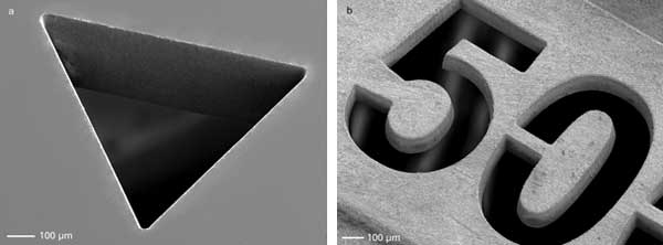
Ultrashort-pulse-width lasers enable precise materials processing, which can yield systems with improved performance. Here, close-ups show what’s possible with sapphire (a) and ceramics (b). Photo courtesy of Trumpf.
Ultrafast lasers are also used for imaging inside the brain through a multiphoton process, said Magnus Bengtsson, director of strategic marketing at Santa Clara, Calif.-based laser maker Coherent. “The trend there is longer wavelengths or multiple wavelengths out of the laser boxes.”
Longer wavelengths offer imaging from deeper inside tissue, since absorption decreases as wavelengths increase. This push toward longer wavelengths is being driven and enabled by the development of suitable fluorophores and laser sources.
Ultrashort-pulse-width lasers also can play a role in sustainable manufacturing, said Sascha Weiler, microprocessing program manager at Trumpf North America of Farmington, Conn., which produces a range of pico- and nanosecond-pulse lasers in the UV, green and IR. Its femtosecond-pulse lasers are all IR.
The ultrashort-pulse laser contribution to sustainability can be seen in products from Robert Bosch GmbH, the Gerlingen, Germany, auto components supplier. Thanks to such lasers, Bosch can precisely drill complex holes into a direct-injection valve for a gasoline engine, which contributes to more efficient combustion and fuel savings of up to 20 percent. Researchers from Trumpf, Bosch and the University of Jena collaborated on the project, and they are up for a German Future Prize for industrial innovation.
Of course, there’s the sustainability of the laser itself to consider, and wattage is important there, Weiler said. “The higher the power, the less costly per watt, and the more efficient the laser processing becomes.”
A trend toward higher power can be seen in picosecond lasers. Trumpf products of this type have moved from 30 W of average power in the green in 2009 to 100 W today, and Weiler expects this upward trend to continue.
Growth in laser power and efficiency is important for additive manufacturing, which constructs parts by adding material instead of removing it. Examples of this technique can be found in advanced aerospace engines, where studies have shown that material and weight savings of up to 80 percent are possible. The technique also allows the manufacture of complex shapes that can improve overall fuel efficiency.
“Additive manufacturing is a pretty hot area, and that’s something lasers are clearly enabling,” said Herman Chui, senior director of product marketing at Santa Clara, Calif.-based Spectra-Physics.
Chui predicted that more additive manufacturing lies ahead, in part because of an expected decrease in laser costs, a consequence of increasing volumes and innovations such as modularization and miniaturization of components.
It’s not yet clear which lasers will be best suited for handling carbon fiber and composite materials. Today these are found in advanced applications such as engine blades and other aerospace components. In the future, they probably will be found in many more products.
It’s likely that processing such materials will take a blend of laser technologies, with some hidden from view. For instance, fiber lasers are a strong trend. So, too, are trends such as lower cost, higher power and application-specific ultrashort-pulse-width lasers. Increasingly, these developments will intersect, said Roland Mayerhofer, innovations manager at laser maker Rofin-Baasel Lasertech in Starnberg, Germany.
“Fiber laser concepts will be more and more present also in industrial ultrashort-pulse-width laser designs,” Mayerhofer said.
San Diego-based Cymer Inc., an ASML company, has a single product focus: laser-based light sources for semiconductor lithography scanners. The company’s 193-nm workhorse powers many of the machines that pattern today’s advanced semiconductors.
That technology is undergoing changes, said Ted Cacouris, director of product management. The semiconductor industry is driving down feature size into the range of tens of nanometers, while the wavelength of the light source remains unchanged. As a result, two or more patterning passes are being used, which has implications for the laser and light source.
“You’ve got to put many patterns on a single layer. So you’ve got to have tighter and tighter overlay as well as having the critical dimension uniformity, or CDU, to be commensurate so you can do that multipatterning,” Cacouris said.
For light sources, that translates into a need for greater uniformity, he added. They fire some 6000 shots a second, each about 130 ns long. Today the wavelength is controlled to tens of femtometers, and the power, which can be as high as 90 W, is controlled to a few percent.
This degree of control is possible, in part, because of sophisticated algorithms for pulse management. Software monitors light sources worldwide from a central control room, and the source parametric data is used by chip makers to predict product yield and performance. All of this data is provided by advanced instrumentation on the light source.
Looking forward, Cacouris sees more of the same. Even when a new light source becomes available, deep-UV scanners – and the light sources that power them – will continue to be used to make chips.
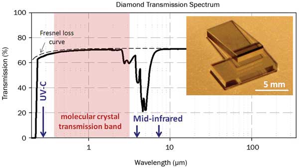
The transmission range of diamond extends from the deep-UV to the far-IR, enabling solid-state Raman conversion to 270, 3500 and 7000 nm. Photo courtesy of Richard Mildren, Macquarie University.
The successor to the 193-nm laser light source is the 13.5-nm extreme-UV source. Getting scanners of this wavelength into manufacturing has been challenging, but progress is being made. Cymer’s extreme-UV source uses a high-power CO2 laser to vaporize a tin droplet. The resulting radiation is a slew of wavelengths, with optics capturing and sending photons of the proper wavelength onto the target.
ASML, which is based in the Netherlands, is committed to hitting something like 100 W of extreme-UV power in 2014. That will enable some 70 semiconductor wafers an hour to be processed, said spokesman Ryan Young.
Key to achieving that number is a double-strike innovation. Hitting the droplet twice, initially with a low-power pulse and then an instant later with a full-power one, allows more radiation to be extracted from each drop. The first pulse vaporizes the tin, producing a cloud that better absorbs the second shot.
The plan is to get to 125 wafers an hour by 2015, Young said. To do that, he added, CO2 lasers with even higher power are needed.
Today the lasers sit at 30 kW, and they might need to go up to 60 kW and beyond. Handling that sort of power as well as the peak power of ultrashort-pulse-width lasers presents a challenge for components in the optical train. One solution might be to employ new materials, such as diamond.
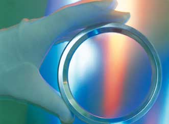
Diamond could be a laser technologist’s new best friend. Large synthetic diamond windows could be useful in high-power, 20+-kW lasers. Courtesy of Element Six.
Element Six, a Luxembourg-registered member of the De Beers Group, produces synthetic diamond. It has been working on this with leading manufacturers of high-power lasers and beam-delivery systems, along with laser technology researchers, said optical business manager Henk de Wit, who noted that diamond is transparent from the near-UV through the IR. It also is strong and the best-known conductor of heat, he added. Those characteristics help in managing high-power lasers.
“You never get a hot spot because all of the heat that is generated is drained off immediately – assuming, of course, that you have proper mounting,” de Wit said. “This means that systems using diamond as optics do not need any compensation technology for thermal lensing.” That makes the system simpler and also easier to shrink, as there are fewer components that have to fit within a given footprint. In making lasers more compact, heat dissipation is important, because shrinking ups the thermal load.
Synthetic diamond has gotten much better in quality, and it could be an important lasing material in the future. Proof
of this concept comes from the University of Strathclyde in Glasgow, Scotland, and Macquarie University in Sydney. At Strathclyde, researchers led by Jennifer Hastie recently demonstrated a multiwatt, continuous-wave tunable diamond Raman laser. When frequency-doubled, the beam is in the orange and could have medical and other applications.
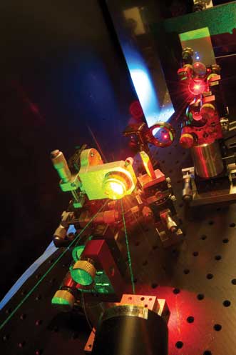
A tunable Raman laser, enabled by diamond, was developed by researchers at the University of Strathclyde. Photo courtesy of University of Strathclyde.
Diamond plays two roles in making this happen, said Alan Kemp, a Strathclyde research team leader. One piece cools the pump, allowing the semiconductor disk laser to run at a higher power; a second piece of diamond Raman-shifts the wave-
length. Adjusting the output of the semiconductor disk laser tunes the Raman laser from 1209 to 1256 nm. In-cavity frequency doubling cuts that wavelength in half.
For this to work, the diamond must be almost perfect. The Raman effect is highly nonlinear, so intensity-robbing material defects play havoc with it. In the case of synthetic diamond, one of the most common possible impurities is nitrogen, which absorbs in the infrared.
Element Six worked with research teams in an iterative material improvement process. The result was an enabling technology and a new lasing material. “The nitrogen is now down to the tens-of-parts-per-billion levels, so the losses are low enough to do serious nonlinear optics,” Kemp said.
At Macquarie University, associate professor Richard Mildren leads a research team investigating both the long and short of diamond Raman lasers. On the short end, a green pump laser interacting with diamond leads to Raman lasing at 573 nm, which can be cut in half through frequency doubling. The result is a high-power continuous laser at about 290 nm, an otherwise hard-to-produce UV wavelength. “UV-C continuous wave is actually quite difficult to generate by other means because [there are] not many gain materials that operate in the visible to enable you to do the intracavity doubling,” Mildren said.
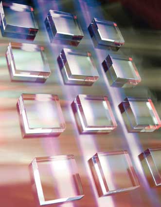
Optical-grade single-crystal synthetic diamond, with its high Raman
gain coefficient, has powered Raman lasers that could offer new
capabilities. Courtesy of Element Six.
On the long end, the Macquarie researchers have used one or two Raman shifts to create lasers in the IR, with wavelengths at about 1500 nm, or 1.5 µm. The group also recently demonstrated lasing at about 3.5 and 7 µm. The lasers pack a punch, with outputs up to 100 W. Conversion efficiency of the pump light is fairly high, once a threshold is passed, Mildren said.
These advances have been enabled by improvements in the quality of synthetic diamond, he added. Thus, the commercial debut of diamond Raman lasers depends upon having enough of the material available, something producers say is now the case.
Finally, for a look at a laserlike technology that may not bear commercial fruit for years, consider research into a new type of coherent source. The concept is based on metamaterials – composites made up of microscopic structures that have electromagnetic interactions and resonances at designed frequencies. Nikolay Zheludev, director of the center for photonic metamaterials at the University of Southampton in England, heads a group investigating this idea.
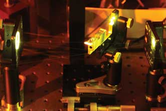
A 2-W diamond laser operating in the yellow at 573 nm. Photo courtesy of Richard Mildren, Macquarie University.
When driven by an electron beam, recent experiments show, such metamaterial-based devices emit spatially coherent and spectrally narrow light similar to that from a laser. The devices are flat, which means that they might be more easily integrated than a traditional laser into a very compact system or onto a chip. Also, a laser is a nonlinear device and may emit no light until a threshold is reached. That’s not the case for the new light source, which Zheludev said would operate at any level of injected power in a linear way.
Although currently pumped with an electron beam, the device also can be pumped optically, he added. This is indicative of phenomena that could be exploited and is found on very small scales.
“At the nanoscale, the conversion from different types of energy – say, light, heat, electric, magnetic – is very, very easy. Also, there’s a complete disappearance between photonics and electronics,” Zheludev said.