Advances in manufacturing and materials will help the military spot targets faster – and from farther away.
For the military, the name of the game is to see first and farthest, which makes optics vital. The length of an optical path can set overall system size, and optical components can fix the weight. Now, advances in materials and manufacturing promise to ease existing constraints.
For instance, more sensors are better. But sensor-laden systems still have to fit in a specific performance, size, weight and power envelope, and those specifications can be tight for systems carried by soldiers or on small unmanned aerial vehicles. Even more challenging is the typical case where sensors scanning different wavelengths require separate optics.
A possible solution to this problem comes from Schott, a multinational optics and coating manufacturer with an Arlington, Va.-based unit serving the US military. Schott has a new family of glasses that could form the basis for multiple-wavelength optics.

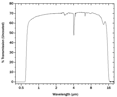
New glasses with transmission from the near- to long-wave IR could enable multispectral optics, cutting the size and weight of sensor packages. The graph shows the transmission based on preliminary data of one of five types of IR glass. Photo courtesy of Schott.
“You can look through our new IR glass, and it’s anywhere from a pale yellow, so transmission starts around 450 nm. Some of these don’t start transmitting until about 550 or 600 nm,” said Matthew Roth, advanced optics business development manager at Schott Defense. “They transmit out anywhere from about 12.5 to 16 µm.”
Thus, these glasses cover some of the visible, the near-IR, the short-wave IR, and the long-wave or thermal IR. The new materials are in prototype right now and consist of four multispectral glasses with differing dispersions at different wavelengths. They enable the building of achromatic lens systems, where light of different wavelengths would be focused together. This allows multiple optical paths to be collapsed into one.
One challenge the company had to overcome had to do with the virtual, rather than the real, material. Standard optical design programs assume that only one wavelength band is being transmitted and so don’t easily deal with two or more transmission bands. To address this, Schott developed software that worked with the new materials.
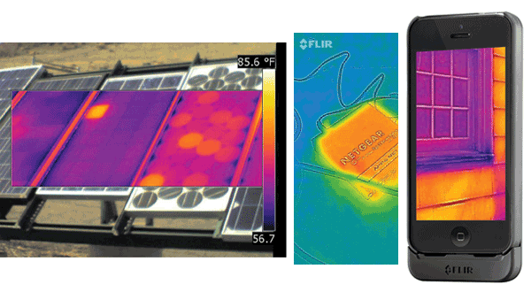
 Thanks in part to optics innovations, the size, weight, power and cost of thermal imagers have been reduced so that smartphones (center) can now see heat and capture multispectral images (left). This advance will eventually find its way into defense applications, allowing less expensive fused visible and IR imaging, as in this solar cell example (right). Photo courtesy of Flir.
As with other long-wave IR glasses, the new materials are chalcogenides. However, they are made from inexpensive raw materials that are less costly than the crystals of gallium arsenide or indium phosphide found in some other long-wave IR glasses. The new glasses also are relatively robust and enable smaller optics because of an index of refraction between 2.0 and 3.0, allowing new capabilities.
“Now you have the ability to do both visible or a near-infrared CMOS and a thermal camera on the same aperture. You’re going to get both a good amount of color information in daylight and a good amount of thermal information,” Roth said.
Schott also is working to cut the cost of packaging optics by changing the process by which molding preforms are made. That development should begin to show up within the year. It will be particularly beneficial to small optics, which must be molded to hit size and weight targets.
Taking full advantage of such optical material advances will require sensor innovations. In particular, a single set of future optics that does the work of two or more current constructs will make demands on sensors. Devices will need dual band function, such as a hybrid that puts both visible and IR sensors on the same focal plane.

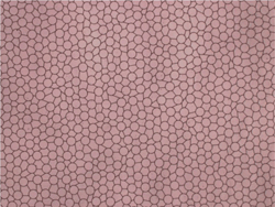
A fine-patterned mesh on sensor windows shields the device from electromagnetic interference while enabling high transmission of visible and IR wavelengths. Photo courtesy of Battelle.
“If you have the optics that can really transmit both wavelength bands, then suddenly you can look at hybridized sensors as well,” said Cees Draijer, senior program manager for defense, security and IR at Teledyne Dalsa of Waterloo, Ontario, Canada.
The camera maker is investigating how this might be done using an uncooled IR sensor. Such an approach would sacrifice some sensitivity and range in comparison to a cooled device, but would cut power requirements. A single set of optics and a low-power hybridized device capable of meeting visible and IR needs could be suitable for deployment on either a soldier or a small unmanned vehicle. Research into and development of multiband sensors was funded by the Department of Defense in DARPA’s DUDE and MONTAGE programs. Started years ago, these projects sought – and reportedly succeeded in creating – a combination near- and long-wave IR sensor on a single chip.
Long-wave IR sensor maker Flir Systems of Wilsonville, Ore., has a sensor development that promises to reduce system size, weight, power and cost, partly resulting from optics innovations. The company’s just-announced Lepton long-wave IR camera module is as small as – and, in volume will cost about as much as – the visible camera module in phones, said Andrew Teich, Flir president and CEO.
Part of the lower cost of the new device is the result of wafer-scale optics technology and optical material choices. In order of expense, the detector, lens, processing electronics and packaging drive the cost of an IR sensor, Teich said. For the new module, Flir uses wafer-scale optics, which enables hundreds or thousands of lenses to be processed in a batch.
In another cost-cutting measure, Flir opted not to go with relatively expensive germanium or hybrid germanium materials. Instead, it settled on less-costly but slightly lower-performing silicon optics.
The uncooled IR detector has a shorter sensing range than Flir products that are cooled. Even so, the new camera module can spot heat differences of a few tens of millikelvins. It has an 80 × 60 pixel array and a 50° field of view. The module could be useful for short-range situational awareness, such as monitoring the perimeter of a forward-deployed camp.
“The 50° field-of-view product has a detection range of about 150 ft for a human target,” Teich said. “The wafer-scale optics technology does have the ability to do narrower fields of view; for example, going to 2× magnification is very doable.”
Initially, the new module is targeted at consumer markets, with one application being a smartphone thermal imaging accessory. But the technology will make its way into defense applications as well. In a way, this illustrates an important trend, where innovations and advances may increasingly arise from consumer markets and then be adapted to military applications.
Another example of optics innovations comes from L-3 Communications’ Applied Optics Center in Dallas. The company designs and manufactures optical thin-film coatings in volume for the defense market and is pushing into other areas, said Jim Hooker, business development manager. He added that most of the military products are in the form of sighting systems.

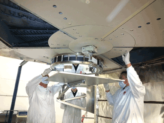
Technicians position a large collimating telescope mirror for coating. Advanced coatings improve optical performance for commercial and defense applications. Photo courtesy of L-3 Communications.
The wavelengths of interest range from the ultraviolet, through the visible and into the IR. Typically, what is desired is a bandpass, with a swath of spectrum as narrow as 5 to 10 nm wide being allowed through and everything else rejected. This performance objective is met by depositing successive layers of thin films and coatings on a substrate.
A relatively simple example of this might be three to five layers, as would be done to create an antireflection coating on glass. More complex would be 40- to 80-layer coatings, aimed at more-exacting light management. “Then there are companies like the Applied Optics Center that are able to deposit in excess of 250 discrete layers for very tight tolerance, precision films,” Hooker said.
The challenge is to do this at the right price while maintaining performance during assembly of the final product, he added. One way to make this easier is to bring coating expertise to bear earlier in the design process. L-3 Communications, therefore, now increasingly offers its know-how to engineering groups as far upstream in the design process as possible.
Optics and coatings of a different sort are powering advances coming out of Battelle, a research organization based in Columbus, Ohio. The first will help the military see while sensors stay protected and undetected; a second is aimed at securing communications.
Sensors must be protected from the battlefield, and that includes the effects of electromagnetic interference. The challenge is that this protection can’t interfere with transmission across a stretch of spectrum. It also must handle a variety of substrates as well as large, curved surfaces.
Battelle has solved this problem, said Philip Schofield, manager of sensors and communications systems. “We apply, using contact lithography, a fine conductive coating over the surface of a sensor window that provides improved EMI [electromagnetic interference] protection.”
For communications, the company is working on implementing quantum key distribution (QKD) schemes. This is based on photon-dependent physical encryption, and so is immune to computation advances that could crack current encryption. Popular QKD schemes depend upon fiber optics, which ferry entangled photons between locations. Distances must increase, however, and that could entail the use of new materials.
Ideally, general advances in defense optics will allow an ever-widening scope of missions, Schofield said. Next-generation, innovative materials could prove vital to developing such capabilities by reducing size, cutting weight and eliminating cost. Some of those advances might involve devising new ways to use well-known materials, such as plastics, that may lack needed performance characteristics.
“Are there coatings that you can put on lower-mass optics that can replicate the performance you get out of shaped optics of much heavier weight or very expensive substrate materials?” Schofield mused.