“Greening” Your Flat-Screen TV
TEL AVIV, Israel, Sept. 7, 2010 — Researchers at Tel Aviv University developed an environmentally friendly organic LED light source for home electronics, medicine and clean energy.
The new light source applies a discovery in nanotechnology based on self-assembled peptide nanotubes to "greening" the optics and electronics industry. Nadav Amdursky, a doctoral student, and Gil Rosenman, a professor in the university’s department of electrical engineering, say their technology could make flat-screen TV production “green” and could even make medical equipment — such as subcutaneous ultrasound devices — more sensitive.

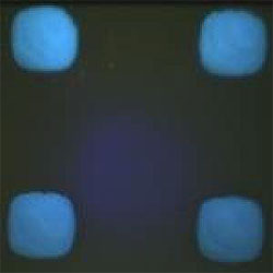
Organic LED light created in the Tel Aviv University lab.
Electronic products are known to pollute the environment with heavy metals before, during and after use. In the US alone, an estimated 70% of heavy metals in landfills comes from discarded electronics. Environmental costs are likely to increase as flat-screen TVs become larger and less expensive.
The scientists were inspired by a biomaterial involved in Alzheimer's disease research, which was discovered by Ehud Gazit, a professor at the university. They developed a new nanomaterial, applying both biology and physics. This biological material is the basis for their new, environmentally friendly variety of LEDs used in consumer and medical electronics.
The invention is more than a clean, green way to create light, the researchers say. It also generates a strong signal that can be used in other applications in the nanoworld of motors, actuators and ultrasound.
"We are growing our own light sources," said Amdursky, who worked under Rosenman during the project. The organic nanolightsticks that they developed using organic chemistry are made from carbon, which makes them cost-effective as well as environmentally friendly.
Unlike conventional light sources, the biologically derived light source has a nanoscale architecture, which facilitates integration into light-emitting devices such as LED TVs and improves the resolution of the picture. The team has recently written a patent to cover the technology.
According to Amdursky, the light emitted by the lightsticks is not appreciably different from the light that emanates from today's inorganically engineered LED lights.
"We don't need a special plant, bacterium or a big machine for growing these structures,” he said.
The core technology and structures, which are described in Advanced Materials, Nano Letters and ACS Nano, exhibit "piezoelectric characteristics," which are necessary for the development of tiny nanoultrasound machines that could scan cells from inside the body. Piezoelectric motors or actuators are only dozens of nanometers wide, which can lead to their application in energy-harvesting systems as supercapacitors — large energy-storage devices, necessary for the solar energy and wind energy businesses.
For more information, visit: www.eng.tau.ac.il
Published: September 2010