Enhancements in optics and image sensor technologies, coupled with the huge increase in computational processing power, allow us to observe and record more features of the universe than ever before. Application-specific and practical factors alike should be considered in camera and sensor selection.
MARK DONAGHY AND JEAN-EDOUARD COMMUNAL, RAPTOR PHOTONICS LTD.
Astronomical imaging techniques have evolved markedly over the past few decades. Astronomers are early adopters of camera technology, pushing the boundaries of new sensor developments and dapting cameras very quickly to their applications. Digital cameras, as well as opto-electronic systems, play a key role in the advancement of astronomical imaging and adaptive optics research, enabling the
study of the evolution and composition of the cosmos in astonishing detail. Myriad imaging applications, including solar astronomy, exoplanet detection and speckle imaging make specific demands of the optoelectronic system acquiring and recording data. Therefore, one of the most fundamental decisions to be made by a system designer is the selection of the image sensor.
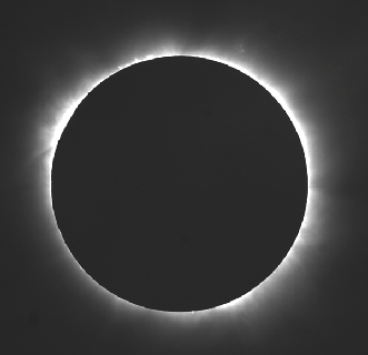
A solar eclipse in Gabon, Africa, on Nov. 3, 2013. Photo courtesy of Philippe Lamy/Laboratoire d’Astrophysique.
A range of available sensors such as CCD, EMCCD (electron multiplying CCD), CMOS (or scientific CMOS) and InGaAs all provide benefits in the wavelength region of interest, be it in the UV, visible, shortwave-infrared (SWIR) or IR region. Different sensors offer various resolutions, pixel sizes, well depths and quantum efficiencies (QEs). The ability to drive the sensor in a camera determines signal throughput, wavelength optimization, readout noise and dark current, as well as readout speed. And all have limitations. There are also more practical issues to consider, including cost, size, interface, weight and ruggedness.
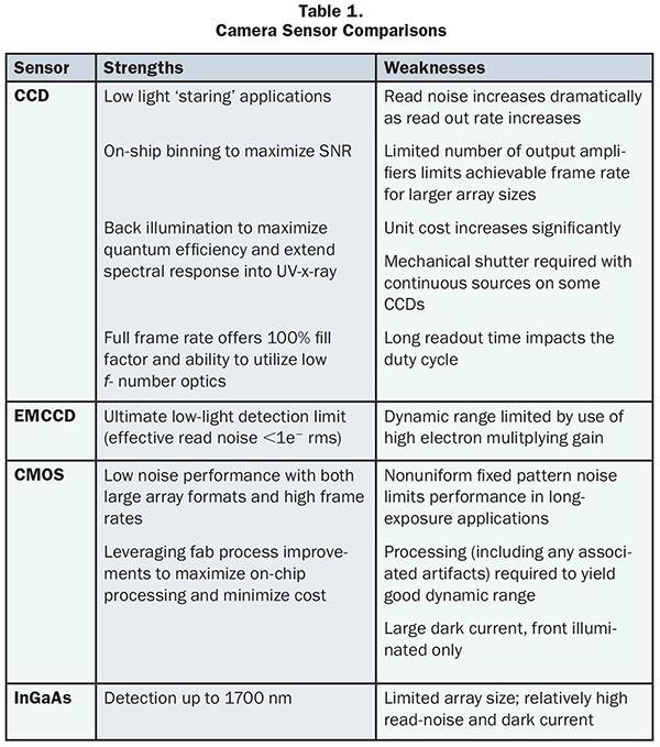
There are a multitude of sensors on the market today, and each comes with a range of properties making it more suitable for a specific application. Table 1 highlights some typical strengths and weaknesses of various sensors.
Sensor types and construction
Construction of a sensor should be a top consideration. CCDs (charge-coupled devices) come in many forms; full-frame CCDs have the simplest architecture. The classic full-frame CCD design employs a single parallel register for photon exposure, charge integration and charge transport. In order to control the exposure and block light from striking the CCD during the read process (which would otherwise result in charge smearing), a mechanical shutter is used. In a full-frame format, the total area of the CCD is available for sensing incoming photons during the exposure period. The format boasts a 100 percent fill factor — each pixel is utilized to detect photons during the exposure. The pixels are typically square, so there is no image distortion inherent to the detector.
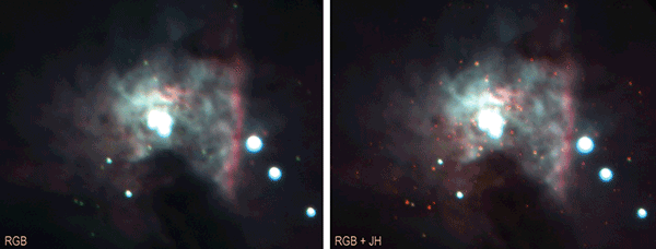
Heart of the Orion nebulae. Photo courtesy of Lyu Abe and Alain Klotz.
A frame-transfer CCD has its parallel register divided into two distinct areas: the image array, where images are focused, and the storage array, where the integrated image is temporarily stored prior to readout. This eliminates the need for a mechanical shutter.
Interline-transfer CCDs (or interline CCDs) have a parallel register that has been subdivided into stripes so that the opaque storage register fits between columns of pixels. The electronic image accumulates in the exposed area of the parallel register. During readout, the entire image is shifted under the interline mask into a hidden shift register. Since the signal is transferred in microseconds, smearing will be undetectable for typical exposures. Interline-transfer CCDs can exhibit relatively poor sensitivity to photons, as a large portion of each pixel is covered by the opaque mask. As a way to increase the fill factor, high-quality interline-transfer devices have microlenses atop the CCD that direct the light from a larger area to the photodiode. This approach raises the detector’s fill factor from approximately 25 percent to >75 percent. This improves net QE across the visible spectrum but limits the ability to optimize wavelengths with on-chip coatings.
While front-illuminated CCD, EMCCD and CMOS are well-adapted for specific applications, large-pixel back-illuminated CCDs are the best choice for visible or near-infrared (NIR) imaging at any exposure, although they are rather costly. Even if a back-illuminated CCD camera is within budget, some applications may be better served using a multitude of observatories equipped with front-illuminated CCD, EMCCD or CMOS cameras for the same price. For observing in the H-band, InGaAs cameras work best. This technology has made great strides in terms of performance and costs, and is now a viable solution for observation.
Wavefront sensors exist in an EMCCD camera equipped with either a microlens array or Shack-Hartmann filters. Low readout noise, fast frame rate and real-time data transfer are crucial. For example, the mWFS setup at the Institute of Astronomy at the University of Hawaii deploys five Shack-Hartmann wavefront sensors (WFSs) over a half-degree field of view to quantify the atmospheric wavefront correlations over extremely large fields of view. Each WFS samples the wavefront from one star in a constellation with 23 × 23,
9-cm subapertures at a rate of 25 to 50 Hz. The wavefront phase correlation and the optical turbulence profile are extracted from the telemetry data. The data from this project is feeding several design studies for ground-layer adaptive optics on Mauna Kea, Hawaii.
It is important to consider whether an on-chip substrate coating is required for the sensor, or a specialized window to reduce reflection or optimize the wavelength band and enhance its transmission. Coatings enhance the ability of light to enter into the detector and be detected, maximizing QE.
Windows coated with fused silica or MgF (magnesium fluoride) will optimize in the UV region, while InGaAs (indium gallium arsenide), InSb (indium antimonide) or MCT (mercury cadmium telluride) are all coatings/alloys that can be applied to CCD or CMOS readout integrated circuits to achieve higher sensitivity in the SWIR region.
Electronic shuttering
Some types of image sensors provide electronic shutter mechanisms such as rolling and global shutter. There are big differences between the two in terms of performance.
In sensors that use a global shutter, all pixels are exposed simultaneously. The entire imager is reset before integration to remove any residual signal in the sensor wells. The wells (pixels) then accumulate charge during the exposure time, with the light collection starting and ending at exactly the same time for all pixels. At the end of the integration period (during which light is collected), all charges are simultaneously transferred to light-shielded areas of the sensor, preventing further accumulation of charge during the readout process. The charges are then shifted out of the light-shielded areas of the sensor and readout. This means that with a global shutter sensor, the scene will be “frozen” in time if the integration time is short enough.
In the rolling shutter sensor, lines of pixels are continuously exposed and read, one after the other. The photodiodes (pixels) do not collect light at the same time. All the pixels in one row of the imager collect light during exactly the same period of time, but the time that light collection starts and ends is slightly different for each row. The top row of the imager is the first one to start collecting the light and the first one to finish collecting. The start and end of the light collection for each subsequent row is slightly delayed. The total light collection time for each row is exactly the same, and the delay between rows is constant. By varying the amount of time between the reset sweeping past a row and the readout of the row, the integration time can be controlled. Rolling shutter integration is not well-suited for capturing short-pulse light sources.
Noise equivalent irradiance, maximizing photon collection
Comparing such a wide variety of sensor technologies can be difficult. It is therefore useful to combine all of them in a single, normalized quantity like the noise equivalent irradiance (NEI), as demonstrated in Equation 1.
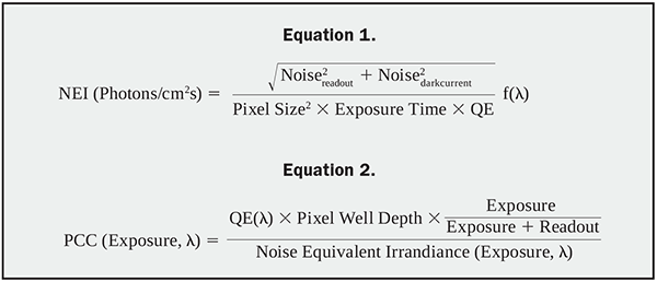
The resulting NEI plot vs. exposure time at different wavelengths allows the selection of the most sensitive technology according to the observation conditions (see Figures 1 and 2).
With the wavelength and exposure time of interest defined, it’s easy to compare a camera’s sensitivity using the NEI.
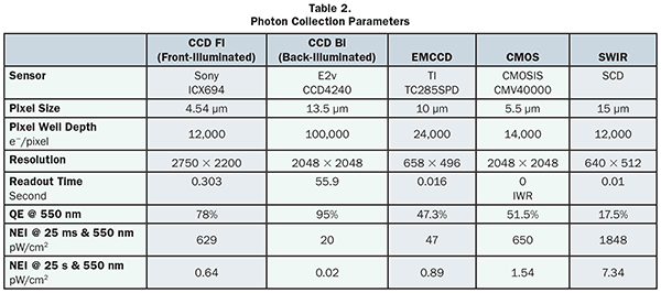
However, one must also take into consideration the pixel size, electron well depth, resolution and readout time. The readout time allows completion of the camera’s duty cycle, which can have a large impact on its efficiency for a short-exposure application, even if it’s extremely sensitive. This is typically the case for large-area, slow-readout-rate, back-illuminated CCD.
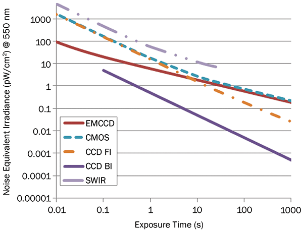
Figure 1. NEI vs. exposure time at 550 nm, visible.
Table 2 details values for front-illuminated CCD, back-illuminated CCD, EMCCD, CMOS and SWIR using specific sensors to give a comparison.
The photon collection capacity (PCC) of a sensor can then be defined as a figure of merit that will be a function of the exposure time and wavelength by taking into account QE, pixel well depth, duty cycle and NEI.
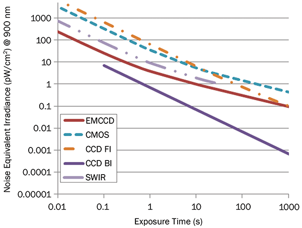
Figure 2. NEI vs. exposure time at 900 nm, NIR.
With the PCC at 550 nm (Figure 3), it is evident that at short exposure, <100 ms, EMCCD are best followed by CMOS (due to their high duty cycle), and front-illuminated CCD and back-illuminated CCD, which both have low duty cycles. Above a few seconds, CCDs are best followed by EMCCD and finally CMOS, which suffer from a high dark current.
As shown in Table 2, with PCC at 900 nm in the NIR, the SWIR camera is starting to perform honorably compared to other technologies. Above 1000 nm, the silicon detector will be useless, and only InGaAs will remain.
Traditional astronomy imaging is done using long exposure times in order to accumulate enough signal, but there are some applications where short exposure time and high frame rate are desirable — the observation of transient events or in order to limit the effect of atmospheric turbulences.
Observations
Observing transient events such as eclipses, transits and occultation naturally puts a limit on the maximum possible exposure time. Dark current becomes a secondary concern behind readout noise and readout time. In addition, the precise recording of the time stamp of the acquisition with respect to Coordinated Universal Time (UTC) is a critical parameter for later data analysis of the image acquired from different observatories. Using a GPS to provide a trigger signal to the camera allows it to achieve <50-µs precision on the image acquisition with respect to UTC.
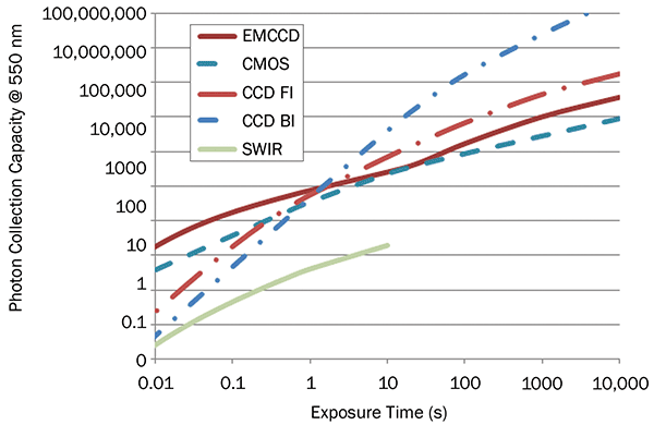
Figure 3. Photon collection capacity at 550 nm vs. exposure.
Establishing the orbit of near-Earth objects is made more precise when their positions can be measured closest to Earth. Again, high sensitivity at short exposure, fast readout and precise time stamp of the acquisition are critical.
Speckle imaging captures a large number of images with short exposure time (typically tens of milliseconds). The goal is to “freeze” atmospheric turbulences in each single frame and process the stack to improve the resolution on the resulting
images. This is a cheaper, simpler alternative to adaptive optics that is becoming more practical thanks to large storage
and processing capacity. It requires cameras with high frame rate and low readout noise.
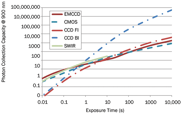
Figure 4. Photon collection capacity at 900 nm vs. exposure.
Double star observation uses speckle imaging to improve resolution and examine relative motion to determine if the they are binary or simple optical doubles. Typically, binary star measurements require more advanced processing techniques than simple shift-and-add autocorrelation and intercorrelation. EMCCDs are ideal since they offer the ultimate sensitivity with fast frame rate, up to 50-Hz full frame and even reaching 150 Hz in 128 × 128 subimage, limiting the dataset size and speeding up the processing. Thousands of images can quickly be acquired in a few seconds and processed easily, yielding very good results with good hobbyist equipment.
InGaAs camera sensitivity in the VIS-SWIR from 400 to 1700 nm allows observation within the IR atmospheric window. Moderately cooled SWIR devices can offer high-performing readout noise — an example is Raptor Photonics’ Ninox, which touts <50 e−/p and dark current, <1500 e−/p/s at −20 °C. Such cameras are particularly effective for the observation of star clusters and planetary imaging, as well as satellites or debris tracking. Other potential applications include fireball spectroscopy.
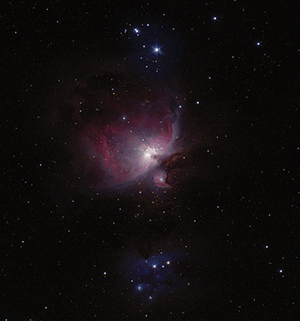
Messier 42. Photo courtesy of Michel Boër and Alain Klotz.
For classic long exposure where low dark current and high resolution is required, CCD cameras are still the best choice. All-sky observations require continuous acquisition for extended periods. Gathering good data relies on the quality and capabilities of the telescope used, i.e., monitored field × depth.
EMCCD cameras are ideal to observe transient or faint events at video frame rate. They also allow for ultrahigh dynamic range imaging, thanks to the cancellation of the readout noise by the EM gain.
Astronomy equipment has reached a level of performance and cost that allows more observatories to gather larger quantities of data for statistical analysis. So, rather than using one single observatory that is capable of reaching the highest magnitude, it has become more viable to utilize several, even if they each only reach a lower magnitude. Together, a swarm of observatory telescopes is capable of more cumulated observation hours and data collection.
There are many variables to consider when choosing the right camera for the right application. Only some of the available options and applications have been discussed in this article. A thorough understanding of the imaging needs will help to quickly narrow down the sensor and camera requirements, taking into consideration physical space and budget constraints.
Meet the authors
Mark Donaghy is vice president of sales and marketing at Raptor Photonics Ltd. in Larne, Northern Ireland; email: [email protected]. Jean-Edouard Communal is sales manager at Raptor Photonics. He has a PhD in physics from Trinity College, Dublin, and is a keen amateur astronomer; email: [email protected].