Richard D. Crisp and Giles Humpston, Tessera Inc.
Solid-state image sensors come in two variants:
CCD and CMOS. CCDs generally offer superior image quality. However, CMOS dominates
in manufacturing volume because it permits an integrated solution in which both
the imaging device and processing electronics can be fabricated in a single die.
The vast majority of CMOS image sensors are front-side illuminated;
i.e., the light from the scene to be imaged falls on the processed face of the semiconductor.
Another variety is back-side illuminated, where the die is mounted inverted and
the light falls on the unprocessed face of the semiconductor. This configuration
yields performance comparable to CCD imagers but with higher manufacturing cost
and more complex packaging requirements. Recent breakthroughs in semiconductor processing
and wafer-scale packaging techniques make back-illuminated image sensors attractive
candidates for higher-resolution imagers on mobile platforms, where small size and
good light sensitivity are highly prized.

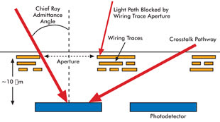
Figure 1. This schematic cross section
is through a front-illuminated CMOS image sensor. For reasons of physics, the photodetectors
are buried ~10 μm deep in the silicon. The wiring trace that connects to each
pixel is built on the surface of the wafer and carefully routed to minimize pixel
obscuration. The resulting aperture influences the maximum angle of captured incident
light and gives rise to a potential crosstalk mechanism. Images courtesy of Tessera.
CMOS imager design trade-offs
The cost of a camera module is directly proportional to two size
metrics: the diagonal of the imager die and the diameter of the optics. Image sensors
from only a few years back had pixel dimensions of tens of microns. In 2009, 1.4-μm
pixels were considered standard, and most sensor manufacturers had road maps out
to 0.9 μm. However, small pixels exhibit poor performance in low-light environments.
There are three reasons for this:
1. Reduced light collection area of each pixel. All other factors
being equal, a large pixel will collect more light flux than a small pixel, resulting
in a better signal-to-noise ratio in the image.
2. With a CMOS image sensor, off-axis light rays are blocked by
the aperture formed by the dielectric and wiring layers above the pixel (Figure
1). The smaller the pixel, the proportionately smaller the unobscured window, allowing
less light through to the photodetector.
3. The vertical separation between the wiring aperture and the
photodetector forms an optical tunnel that restricts the field of view of each pixel.
This is termed the chief ray admittance angle and is most acute for small pixels.
Unless the optics are configured so that light falls on the image sensor at a perpendicular
angle, light-collection efficiency will fall off, particularly at the sensor edges.
The required telecentric lenses are generally incompatible with cheap, compact optical
trains because the train requires the rear optical surface to be both large diameter
and large radius of curvature.
Back-illuminated CMOS image sensors
CMOS back-illuminated image sensors largely solve the above problems.
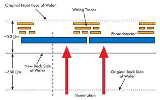
In this configuration, the wiring trace is underneath the photodetector (Figure
2). The entire area of each pixel can be used for photon capture with no restrictions
on the chief ray admittance angle and almost complete elimination of adjacent pixel
optical crosstalk. Although a typical front-side-illuminated image sensor has a
quantum efficiency (QE) – the effective conversion of photons to electrons
– of 20 percent, the QE of a back-side illuminated imager can exceed 80 percent.
This performance gain can be used to dramatically boost low-light sensitivity or
to reduce imager size. For example, reducing a 2.8-µm pixel (at 20 percent QE) to
1.4 µm (at 60 percent QE) results in the same sensitivity but decreases the area
of a corresponding VGA imager by 62 percent.

Figure 2. In this schematic cross section through a back-illuminated CMOS image sensor,
the die is fabricated in the conventional orientation, but the bulk silicon is then
removed, exposing the photodetectors. Making the photodetectors large and easily
accessible trades manufacturing cost against performance and/or size.
Visible light can penetrate only a short distance into silicon.
Therefore, to expose the photodetectors in a back-illuminated CMOS sensor, the majority
of the original wafer thickness must be removed. The thinning uniformity must be
extremely precise because excess silicon presents an effectively opaque barrier.
Thickness variation manifests itself as sensor shadowing, and high average thickness
will render the sensor unresponsive. Clearly, there also are basic handling and
yield issues with 30-mm-diameter silicon wafers that have been thinned to 20 μm.
A simple way to accurately control wafer thinning is to fabricate
imagers on silicon-on-insulator (SOI) wafers because the buried oxide layer provides
an effective stop for the silicon etch. The drawback of this approach is that these
wafers are more expensive than conventional device-grade silicon. However, SOI wafers
also provide a less obvious benefit that makes their use as the starting material
for CMOS back-illuminated image sensor manufacture rather attractive.
 Achieving high quantum efficiency and wide dynamic range from
a photodetector essentially requires keeping dark leakage current low and efficiently
collecting charge generated by photon absorption. Both goals can be accomplished
with an accumulation layer in the form of a p-type surface doping. A simple way
to do this is to exploit the SOI wafer structure. Before sensor fabrication, the
device layer of the SOI wafer is doped with a heavy p-type element at the interface
to the buried oxide layer. The various heat treatments during device fabrication
will activate and redistribute the impurities, forming the desired surface accumulation
layer when it is exposed by the etch process.
Back-illuminated CMOS image sensors are not without problems.
But a general truism is that they provide improved imaging performance for increased
die cost.
Back-illuminated CMOS image sensor packaging
As with their front-face counterparts, back-illuminated CMOS image
sensors require a cavity package for their function and longevity. However, packaging
of back-illuminated image sensors poses special challenges, not least because the
die are used inverted, so the bond pads face the package substrate and are therefore
inaccessible.

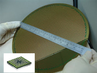
Figure 3. This imager die, housed in a wafer-scale package, uses
a low-cost via-through-pad interconnect to connect the die bond pads to the package
lands and the ball grid array interface. It is based on polymer technology with
a single redistribution layer for the wiring trace, making it very low cost and
highly reliable compared with other variants of through-silicon via.
The generally adopted solution is to use through-silicon via technology
to connect the bond pads to new lands on the optically active face of the die. The
die then can be wire-bonded in the conventional manner. The principal objection
to this arrangement is cost because it entails implementing two interconnect technologies.
A preferred solution is to use a wafer-scale package with a ball grid array interface
so that the contacts remain underneath the die and do not have to pass through it.
A modern wafer-scale package for image sensors is shown in Figure 3. The package
thickness is approximately 500 μm, making it eminently suitable for electronic
products where the current fashion is for extreme thinness.
Conclusion
Back illumination offers the prospect of a new generation of mass-produced
CMOS image sensors for both optical and nonoptical imaging. It permits a significant
improvement in quantum efficiency, which can be used to reduce pixel size. The ability
to manufacture small pixels permits imager resolution to increase while the size
of the resulting camera module decreases.
Back-illuminated image sensors are preferably housed in wafer-scale
packages that use via-through-pad interconnects to a ball grid array interface because
this arrangement obviates the need to use costly through-silicon vias. The primary
application is likely to be higher-resolution cameras for mobile platforms, where
the increased imager cost can be borne, with camera size being paramount.
Meet the authors
Richard D. Crisp is the director of semiconductor technology and
applications, and Giles Humpston is the director of applications, both at Tessera
Inc.; e-mail: [email protected]; [email protected].