The ultraviolet region of the spectrum comes with unique coating challenges, but choosing the right coating technique can optimize the optics for the application at hand.
Alan Graham and Stephen Vincent, Agilent Technologies
Over the past decade, thin-film coating technology and designs have improved significantly, resulting in lower-loss filters and in mirrors that are more spectrally accurate and that perform better under a variety of operational environments. In the previous decade, state-of-the-art evaporation chambers were limited to much fewer than 100 coating layers; now with the improvements in ion-assisted deposition and sputtering, key process metrics (i.e., pressure, temperature and deposition rate) can be controlled with sufficient precision to enable thin films with several hundred coating layers.
However, most coating development has focused on the visible and near-infrared regions of the spectrum. The UV region presents unique materials, fabrication and coating challenges. UV-wavelength excimer lasers and lamp sources are driving high-volume requirements for optical components, especially mirrors.
The term “ultraviolet” — from the Latin “ultra” for “beyond” — refers to light with a wavelength shorter than the shortest wavelength of visible light, generally accepted to be ~400 nm. The UV spectrum commonly is subdivided into several overlapping regions (Figure 1).

Figure 1. The UV part of the optical spectrum includes deep-, extreme-, vacuum- and near-UV wavelengths.
The various UV subspectra have their origins in physics (i.e., “extreme-UV” photons interact mainly with inner shell electrons and nuclei versus interactions with the chemical valence electrons above ~30 nm) and in application (i.e., “vacuum-UV” photons are strongly absorbed in air, and, thus, are historically used in vacuum). The resulting hodgepodge of definitions makes it difficult to identify requirements and to implement solutions across broad regions of the UV spectrum. So for simplicity, we refer to two regions of the spectrum driven by available coating technologies and materials: the near-UV, for wavelengths between 220 and 400 nm, and the deep-UV, for wavelengths below 220 nm.
Applications in the near-UV subspectra include micromachining, thin-film transistor annealing, remote sensing, DVD mastering, microlithography and remote sensing. Although micromachining applications also exist in the deep-UV, the applications in this region of the spectrum are predominantly photorefractive keratotomy and leading-edge semiconductor photolithography systems.
Coating materials, techniques
Evaporative coatings rely on a process whereby the coating material is converted to its vapor state at an elevated temperature in a vacuum chamber. Coating materials (oxides or fluorides) condense on the optical substrate — and everywhere else — in clumps. Clumping can be reduced by heating the substrate, thereby increasing the mobility of the atoms. Doing so also improves adhesion to the substrate, although the atoms still form “islands” that join together, creating zones of separation that result in a low packing density (Figure 2a).

Figure 2. Electron beam deposition, ion-assisted deposition and sputtered thin-film techniques all produce different packing densities.
Although electron beam-deposited thin films have a high-energy damage threshold and low mechanical stress, the zones of separation allow water vapor and other contaminants to penetrate the film. The adsorption of water vapor increases the thin film’s optical thickness, resulting in a shift in the spectral performance. Spectral shifting can be reduced by increasing the film’s packing density (Figure 2b) using ion-assisted deposition, but an increased packing density also increases mechanical stress and reflected wavefront distortion.
Sputtered coatings use a plasma to knock molecules from a solid target material (typically oxides, sub-oxides or metals) through bombardment by energetic ions, eliminating the need for high temperatures. The packing density (Figure 2c) of sputtered thin films approaches that of bulk material, resulting in an environmentally stable coating. Process controls available with sputtering chambers enable a wide variety of complex coating designs of hundreds of layers, improving the overall optical performance.
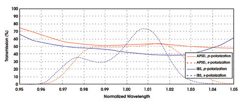
The inherent stability of deposition rate and the relatively high adatom energy of sputtering processes such as ion-beam sputtering enable a more consistent layer thickness and thin-film index control than traditional evaporated or evaporated ion-assisted deposition films, although the deposition process is slow and expensive. Newer sputtering technologies, such as advanced plasma sputter deposition, improve upon the uniformity and layer-thickness accuracy advantages of ion-beam sputtering but with volume throughput similar to that of traditional evaporation techniques. This combination of advantages results in better-performing yet lower-cost thin-film designs (Figure 3).

Figure 3. The performance of immersed, nonpolarizing beamsplitters is shown for ion-beam sputtering (IBS) and for advanced plasma sputter deposition (APSD).
Unfortunately, the high-energy ions in sputtering processes cause fluoride atoms to separate from the metal atoms in fluoride coating materials (fluorine disassociation), producing toxic fluorine gas and metal atoms. The fluorine gas will be pumped out of the coating chamber, leaving a metal atom embedded in the film structure. The higher content of metal in the metal fluoride thin film significantly increases light absorption, which not only reduces the optical efficiency but also can cause catastrophic failure through other mechanisms.
As films become thinner in the UV, their behavior becomes increasingly sensitive to factors such as substrate surface state, material purity and process cleanliness. Defects at interfaces and within the films lead to undesirable optical and mechanical properties. Additionally, the mechanical stress induced by the higher packing density of sputtered thin films typically causes the reflected wavefront distortion to be higher than that of ion-assisted deposition coatings.

When the coating material choices are unconstrained, mechanical stress can be mitigated by matching the coating materials and their associated evaporation parameters. Where the coating materials are limited, additional methods must be used to compensate highly stressed films. In particular, when the ratio of the substrate diameter to thickness is large, the highly stressed thin film can deform the substrate from its design specification. A compensating film on the opposing surface of the optic can be designed such that it “pulls” the optic back into the specified surface figure.
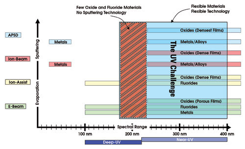
For many applications, sputtering is the best deposition technology. Although sputtered oxide materials often are the solution of choice for thin-film deposition, most oxide thin films are opaque below ~220 nm, leaving fluorides as the primary thin-film material at shorter wavelengths. This combination of constraints enables the UV spectrum to be segmented broadly by materials’ availability and manufacturability into two regions. These are between 220 and 400 nm (near-UV), where oxide materials are available and, thus, sputtering technology is useful, and at wavelengths shorter than 220 nm (deep-UV), where fluorides and electron-beam evaporation typically are used (Figure 4).

Figure 4. The UV spectrum can be segmented by materials’ availability and by manufacturability into the region wherefluorides and electron beam evaporation typically are used and into the region where oxide materials are available and thus where sputtering technology is useful.
An ideal coatings palette
Because oxides and fluorides both transmit between 220 and 400 nm, evaporation and sputtering are viable technologies for deposition at the near-UV wavelengths. Historically, electron-beam deposition has been used for these wavelengths, but environmental shifting resulting from water adsorption has resulted in ion-assisted deposition and in ion-beam sputtering becoming the preferred deposition technologies of choice for many applications.
Ion-assisted deposition is a common upgrade path because it is a modification to existing electron-beam chambers and a cost-effective capital expense. In addition, an ion-assisted deposition chamber uses the same evaporation materials, so it is a cost-effective manufacturing process. Ion-assisted deposition’s advantage is that it produces thin films with near-bulk density, which reduces environmental shift, although at a cost of increased stress and reflected wavefront distortion.
Ion-beam sputtering has been less commonly used because of the capital expenses necessary to outfit a new coating chamber, but with the decline of the telecom market, ion-beam-sputtering chambers have been available on the secondary market, making the capital equipment expense less of a concern. Although the denser films produced with this method increase mechanical stress, the deposition accuracy of ion-beam sputtering enables thinner layers and lower layer count. However, ion-beam-sputtering chambers have higher operational and maintenance expenses than e-beam and a significantly smaller volume throughput.
Newer sputtering technologies such as advanced plasma sputter deposition offer efficient, low-maintenance operation with high-volume throughput. Incorporating the latest optical monitoring technology, advanced plasma sputter deposition can produce a wide range of complex coatings with unsurpassed accuracy and reproducibility.
Designing coatings at the deep-UV wavelengths, including the popular 193-nm wavelength of ArF excimer lasers, is considerably more problematic because the vast majority of oxides absorb below 220 nm and require high layer counts and complex designs that result in a narrow bandwidth that is unusable for most applications. Fluoride thin films for these wavelengths therefore must be manufactured using electron-beam evaporation; because of the wavelength and photon energy, the coating layer accuracy is considerably more important than it is at visible and near-IR wavelengths — you pay an exponential price below 220 nm for “sloppiness.”
Broadband lamp-based applications present a real problem because their requirements span the near-UV/deep-UV classifications and require both oxides and fluorides. Research is under way to determine whether advanced plasma sputter deposition can be used to address requirements from 400 to below 200 nm.
So the ideal optical coating solutions palette includes access to the three key deposition technologies (electron beam, ion-assisted deposition and sputtering — preferably high-volume throughput), stress-compensation techniques, and the process control equipment and knowledge necessary to yield the best results with each method. A continuing investment in capital equipment and development to maintain cutting-edge capabilities is essential to using any of these technologies successfully.
Coating technology is evolving rapidly, with new tools and better metrology available to create and measure the much thinner-layer structures in the near-UV and deep-UV regions. Knowledge and experience with fluoride and oxide coating materials, with all of their idiosyncrasies, allow creation of innovative designs for given applications. Characterizing and measuring the resulting thin-film coatings are essential to ensuring consistent quality and process control. Partnering with a successful company that can engage in design and rapid prototyping — including specification engineering, stringent design and manufacturing tolerances — will ensure the best possible thin-film coating outcome for any given wavelength region.
Meet the authorAlan Graham is the business development manager, and Stephen Vincent is the optical thin films research and development engineer for Agilent Technologies’ precision optics and assemblies business, based in Santa Clara, Calif.; e-mail: [email protected].