GaN-based microdisplays are one of the best candidates to achieve the high brightness and resolution augmented reality systems require.
FRANÇOIS TEMPLIER, CEA-LETI AND III-V LAB
The growing interest in wearable devices has highlighted the need for high-performance microdisplays. Such displays are based on technologies that include reflective or transmissive liquid crystal displays (LCDs), organic LEDs (OLEDs) or MEMS-based devices such as micro-mirror arrays for digital light processing and laser beam steering.
Emissive microdisplays based on OLEDs are particularly attractive for these applications; each pixel is self-emitting, resulting in low power consumption, high compactness and producing excellent image quality. However, for applications such as see-through glasses, a brightness of 5000 cd/m2 or more is needed, which exceeds the possibilities of current OLED microdisplays. At the same time, there is a need for high-brightness emissive microdisplays for compact, handheld projectors and small head-up displays.

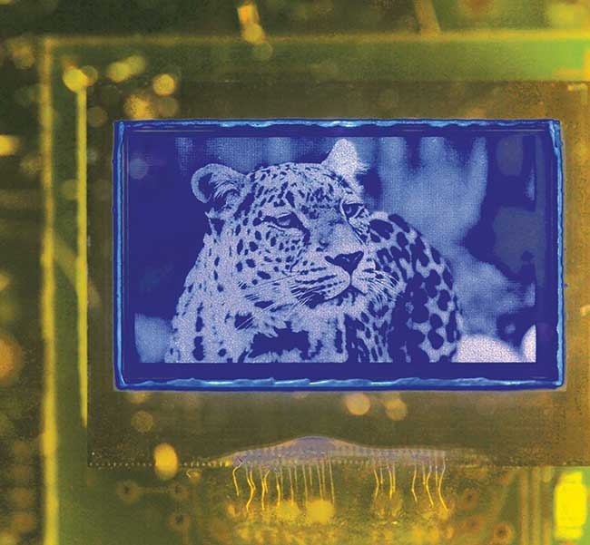
Image obtained on a blue active-matrix WVGA (wide video graphics array) microdisplay. Courtesy of CEA-Leti.
Group-III nitrides composed of GaN and its alloys with InN and AlN were a breakthrough in the lighting market because of their outstanding performance and capacity for emitting a wide range of wavelengths in the near-UV and visible spectrums. These materials were also proposed for high-brightness microdisplays, and in 2011, a full-resolution active-matrix III-N display was demonstrated1.
Since then, a number of players in the field have emerged, ranging from academic research to public or industrial R&D labs and startup companies. A significant increase in publications, announcements and demonstrations of GaN-based microdisplays — particularly in the last two years — has also occurred.
Conventional fabrication techniques
The main challenge for GaN microdisplays is in fabricating them.
A display consists of an electronic driving circuit — called an active matrix — that supplies the desired electrical signal to each pixel, and an electro-optical element that converts the electrical signal into visible information in the form of photons. In all existing display technologies, namely LCDs, OLEDs and e-paper displays, the active matrix is the first element fabricated. Then the electro-optical part is directly processed on top of it at temperatures the CMOS active matrix can withstand, which are lower than 400 °C.
In the case of GaN microdisplays, it is not possible to apply this flow, since GaN material is deposited at temperatures higher than 900 °C and cannot be deposited directly on top of the active matrix. Therefore new approaches are required.
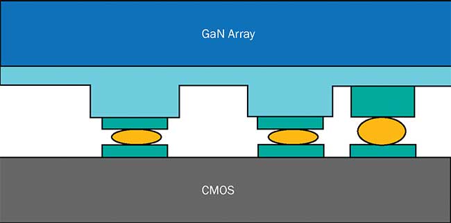
The most straightforward method is hybridization (Figure 1), which has been used by most GaN-based microdisplay developers throughout the past few years. The technique involves fabricating the GaN microLED array on one side, then fabricating the silicon active matrix on the other, and hybridizing them. Hybridizing consists of coupling the two parts mechanically and electrically. This involves alignment and assembly, where each individual LED pixel should be electrically connected to the corresponding driving pad (in general, the anode side) of the active matrix, and so should the common electrode (generally, the cathode). Achieving a very small pixel pitch using this approach requires fabricating the LED array on sapphire with the desired small pitch and developing hybridization technology compatible with this pitch.

Figure 1. Principle of hybridization technology for GaN microdisplays. Courtesy of CEA-Leti.
A particular difficulty with hybridizing the GaN LED array and CMOS active matrix is its need to be performed at a low temperature, due to the mismatch of substrate coefficient of thermal expansion (sapphire vs. silicon). In the meantime, a small pixel pitch is desired for microdisplay applications — namely 10 µm and less.
Classical hybridization techniques such as bump flip-chip technology, however, are not compatible with a pixel pitch of 10 µm or less. The state of the art for display applications is 15 µm1.
A new technique combines low-temperature operation to ensure compatibility with heterogeneous substrates and a pixel pitch of 10 µm and less2.
Recent demonstrations have shown that it is possible to hybridize heterogeneous devices at a pixel pitch of 10 µm using this method, making it suitable for LED microdisplay fabrication. The principle of this technique (Figure 2) is to grow microtubes on the pads of the silicon circuit and align/couple the circuit with the GaN array; the microtubes are then inserted in the GaN arrays pads.

Figure 2. Microtube grown on silicon circuit (a), schematic of hybridized LED array on silicon circuit with microtube technology (b). Courtesy of CEA-Leti.
Leti and III-V Lab recently developed active-matrix, wide video graphics array (WVGA) (873 × 500-pixel) GaN microdisplay prototypes fabricated with microtube technology.
GaN LED arrays are made on sapphire substrates. Each microLED has an anode contact on top and a cathode contact at the bottom. The cathode contact is shared by all the microLEDs of the matrix (common cathode).
Base wafers consist of 4-in.-diameter sapphire with 440-nm or 525-nm LED multiquantum-well InGaN/GaN epitaxial structure grown by metal-organic chemical vapor deposition for blue or green emission, respectively.

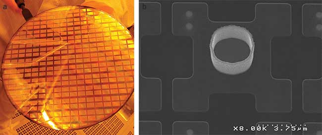
Figure 3. Fabrication of the 10-µm pixel pitch LED array on sapphire. Scanning electron micrograph of the LED array. Inset shows a cross section of a single microLED (a). Photograph of a fully processed wafer with ~100 microLED arrays (b). Courtesy of CEA-Leti.
The GaN array fabrication process consists of depositing and patterning the P-contact metal pads, and patterning the pixels by etching GaN stack using plasma process (Figure 3). Then metal is deposited between the pixels to make a common cathode, electrically connected at the bottom of each microLED. Finally, pads are deposited on each device, for the further insertion of the microtube. In all, about 100 micro-LED matrices were fabricated on each wafer (Figure 3b).
The finished GaN wafers have a series of ~100 microLED arrays featuring 873 × 500 pixels at 10-µm pitch (Figure 3b). Prior to hybridization, singulation of LED arrays was made by wafer dicing. Active matrices for the 873 × 500-pixel displays were fabricated using conventional CMOS process on 200-mm wafers (Figure 4). Each pixel contact was connected to the anode of each LED.

Figure 4. A 200-mm wafer with CMOS active matrices for GaN 873 × 500-pixel microdisplay at 10-µm pitch (a). Scanning electron photograph of a pixel electrode of the CMOS active matrix with the microtube (b). Courtesy of CEA-Leti.
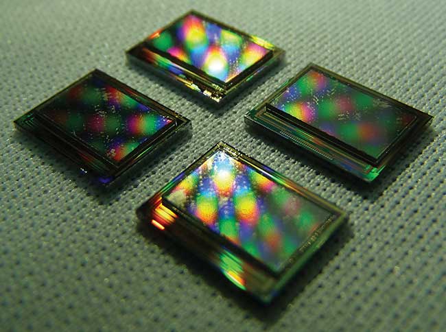
Microtubes were grown on the silicon interconnect for passive displays and directly on full-CMOS wafers for active-matrix prototypes, using conventional integrated circuit process steps (Figure 4b). GaN arrays with 873 × 500 pixels at 10-µm pitch were then hybridized onto the CMOS active matrix (Figure 5), and blue- and green-emitting GaN arrays were fabricated. Active-matrix displays were integrated on a daughter board and connected by wire bonding. The daughter board was then connected to a motherboard.

Figure 5. A hybridized active matrix GaN 873 × 500-pixel microdisplay at 10-µm pitch. Courtesy of CEA-Leti.
The active-matrix WVGA blue and green microLED arrays then underwent electric-optical evaluation. The prototypes feature high resolution and can operate in full video mode. The active-matrix LED microdisplays feature the highest resolution (873 × 500 pixels) with the smallest pixel pitch (10 µm).
In former-generation 10-µm pixel pitch GaN array prototypes, where a selection of pixels were driven directly with high current, the researchers demonstrated extremely high brightness that can be achieved with this method — namely, exceeding 1 million and 10 million Cd/m2 in blue and green, respectively3. In the case of active-matrix microdisplays, the current in each pixel is limited by the CMOS circuit; therefore such brightnesses cannot be reached. Despite this, a level of 10,000 Cd/m2 on the green active-matrix WVGA microdisplays was achieved, which is still a promising result.
Creating color
As of today, GaN-based microdisplays are still not on the market. Several challenges need to be overcome before these displays will be commercially manufactured.
As with all displays, three highly saturated elemental colors (red, green and blue) are needed for each pixel. However, compared with LCDs and OLEDs, conventional thin-film inorganic LEDs fabricated from the same epilayer emit light at a single color (determined by the specific multiquantum well structure used). Such monochromatic emission complicates the development of multicolor devices, which explains why color is the main difficulty for GaN-based microdisplays.
The straightforward way of creating color is to generate the three colors separately with corresponding multiquantum wells. Blue and green emission can be obtained using InGaN/GaN multiquantum wells grown on sapphire. The emission wavelength is set by indium content in the well; blue is obtained with ~10 percent and green is achieved with ~25 percent.
Indium insertion increases defects and, as a consequence, impacts external quantum efficiency. Red can theoretically be obtained with higher indium insertion, but the external quantum efficiency then falls below acceptable levels. To obtain red emission with good external quantum efficiency, other material such as InGaP/InAlP multiquantum wells grown on GaAs are used. Therefore, to generate the three colors, it is necessary to integrate vertically (or laterally) three different multiquantum wells made with different materials. This constitutes a serious technological challenge.
The other solution is to use color converters: using blue emission and down converting it into green or red by photoluminescence using phosphor materials. Using this approach, highly saturated red can be obtained using quantum dots as converters. A difficulty in obtaining a full-color display with this approach is patterning such converters with a small pixel pitch.
The other big hurdle relates to yield and manufacturing. Today, no user accepts pixel defects in a display; therefore, GaN microdisplay fabrication processes will have to gain in maturity to reach the yield target.
In the meantime, fabrication cost must also be considered since the new customers will not accept any price for the upgraded display performance provided by GaN microdisplays.
The microtube hybridization technology is well suited to the specific requirements of microdisplay fabrication. The recent creation of full-active-matrix, high-resolution (873 × 500-pixel) and small-pixel-pitch (10 µm) microLED GaN microdisplays shows that the developed technology is very promising for the fabrication of high-resolution, small-pixel-pitch, high-brightness GaN-based emissive microdisplays.
Meet the author
François Templier is research director at CEA-Leti in Grenoble, France. His research activity is focused on advanced displays,
particularly GaN-based emissive microdisplays, flexible displays and thin-film transistors; email: [email protected].
References
1. J. Day et al. (2011). III-Nitride full-scale high-resolution microdisplays. Appl Phys Lett, Vol. 99, p. 031116.
2. B. Goubault de Brugière et al. (2011). A 10μm pitch interconnection technology using micro tube insertion into Al-Cu for 3D applications. 61st Electronic Components and Technology Conference, IEEE.
3. F. Templier et al. (December 2015). Blue and green 10-µm pixel pitch GaN LED arrays with very high brightness. Presented at the 22nd International Display Workshops 2015.