WAFER TRANSFER
CyberOptics Corp.Request Info
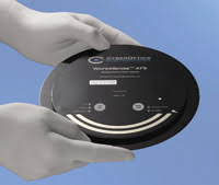 CyberOptics Semiconductor Inc. has unveiled the WaferSense automatic teaching system, a measurement technology for 200- and 300-mm semiconductor process equipment. The wireless and wafer-like device provides accurate wafer transfer coordinates for robotic handling and reduces equipment downtime and wafer scrap. It uses machine vision to “see” targets that mark wafer transfer locations and then transmits their digital coordinates to the operator. A camera captures live video from inside semiconductor equipment as an image processor reports the X-Y-Z offset from the teaching wafer to a target inside the equipment. Software logs data for comparison and analysis and helps to “train” the device to recognize new types of targets.
https://www.cyberoptics.com
/Buyers_Guide/CyberOptics_Corp/c3317
Published: March 2007
REQUEST INFO ABOUT THIS PRODUCT
* First Name:
* Last Name:
* Email Address:
* Company:
* Country:
Message:
When you click "Send Request", we will record and send your personal contact information to CyberOptics Corp. by email so they may respond directly. You also agree that Photonics Media may contact you with information related to this inquiry, and that you have read and accept our
Privacy Policy and
Terms and Conditions of Use.
Register or login to auto-populate this form:
Login
Register
* Required