Two-Photon Polymerization: Additive Manufacturing From the Inside Out
TOMMASO BALDACCHINI, MATTHEW PRICE AND PHONG DINH, NEWPORT CORP.
The 20th century was an era of revolutionary materials science development, as plastics, semiconductors and biomaterials were introduced, and established materials such as metals and ceramics were significantly upgraded. These new and improved materials ushered in countless applications in industries as diverse as electronics, transportation, energy and health care.
In addition to discovering new applications for materials, existing applications can also be improved considerably through better materials. In particular, the desire for lighter or smaller materials — without a decrease in functionality — is a challenge for today’s scientists and engineers. One need only look at the computer industry to see how materials technology has contributed to reducing the size of a machine that once filled an entire room to fit into the palm of one’s hand.
The impending breakthrough applications of the 21st century demand much more than just lighter or smaller materials. They must be stronger, stiffer, capable of damping a range of vibrations or managing heat. Traditional materials science, which has focused mainly at the chemical level, is a mature field and therefore not likely to provide the solutions needed for new applications. Thankfully, a new technology is emerging: microstructured materials.
The concept of a microstructured material can be seen in the macro world. Lattice towers and truss bridges, for example, are dependent not only on the type of materials chosen, but also on the size, shape and placement of the components that make up the entire structure. With a clever design, a tower or bridge can be built with the minimum amount of materials to withstand heavy forces and loads, making them lightweight and strong at the same time.
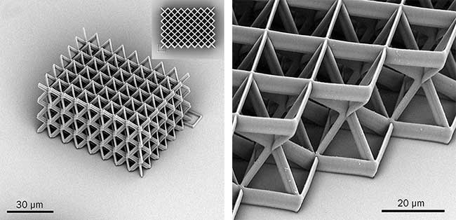
At a microscopic, or cellular, level, a cross section of a microstructured material also looks like an array of trusses (Figure 1). As with a macrostructure like a lattice tower, these trusses can also be designed to provide the material with additional features. Moreover, the architecture of microstructured materials can advance the properties of the ultimate object far beyond what traditional materials science has done at the chemical level. Proper design of microstructured materials can provide more than one functionality, such as high stiffness and damping coefficient. Microstructure design can also decouple properties that typically compete with each other, so it is possible, for example, to have a single material that provides high strength at low density.

Figure 1. Scanning electron microscope (SEM) images of microstructured materials fabricated by two-photon
polymerization (TPP). In (a), the whole pattern is shown at an angle and from a top view (inset). In (b), a magnified view of the unit cell of a microstructured material is shown. Courtesy of Newport Corp.
Microstructured materials are an exciting field, and, like most potentially disruptive technologies in their early stages, they also present challenges. In particular, the manufacture of these complex geometries at the microscopic level is one of the first hurdles researches must overcome.
Two-photon polymerization manufacturing
A promising manufacturing technique for the realization of microstructured materials is two-photon polymerization (TPP). There are two key reasons that render TPP an attractive solution for the fabrication of microstructures. The first is that TPP is intrinsically a 3D writing technique; it does not require a layer-by-layer approach to create complex objects. TPP can also create microstructures with submicron feature sizes in a straightforward manner. These characteristics originate from the nonlinear optical nature of light absorption in TPP and from the chemistry of the polymerization.
In a typical experiment, near-infrared (NIR) emission is used to excite a photosensitive material (resin) that upon light absorption undergoes a phase change from liquid to solid through a polymerization process. Since the resin is transparent in the NIR region of the spectrum, high numerical aperture (NA) lenses and femtosecond pulsed lasers are employed to increase the probability of a multiphoton absorption event to occur. That is, two or more photons are simultaneously absorbed by specialized molecules in the resin (photoinitiators) to create the active species that start polymerization. Under these conditions, multiphoton absorption occurs only in the region where light intensity is the highest. That confines polymerization within the volume of the focused laser beam (voxel). Three-dimensional microstructures are created by precisely overlapping voxels through the scanning of either the laser beam or the sample around predetermined geometries. Successively, the microstructures are revealed by washing away the unsolidified part of the resin using an organic solvent.
TPP offers a unique combination of advantages:
• No topological constraints are present in the fabrication of 3D structures.
• Subdiffraction-limited feature sizes can be attained by employing laser intensities just above the intensity threshold at which polymerization will occur.
• Movable components can easily be fabricated without the use of sacrificial layers.
• The carbon-based nature of the photosensitive materials can be used as a chemical handle to fabricate structures with tunable physical and chemical properties such as hardness, shrinkage, index of refraction and chemical specificity.
It should not come as a surprise then that 3D microfabrication by TPP has evolved in recent years from a novel technique employed mostly by laser specialists to a useful tool in the hands of scientists and engineers working in a wide range of research fields. A perusal of the scientific literature on this topic reveals how extensive the impact of TPP has been in applications that require high-precision 3D writing — from the fabrication of optical and mechanical metamaterials to the development of rationally designed substrates for cell motility studies.
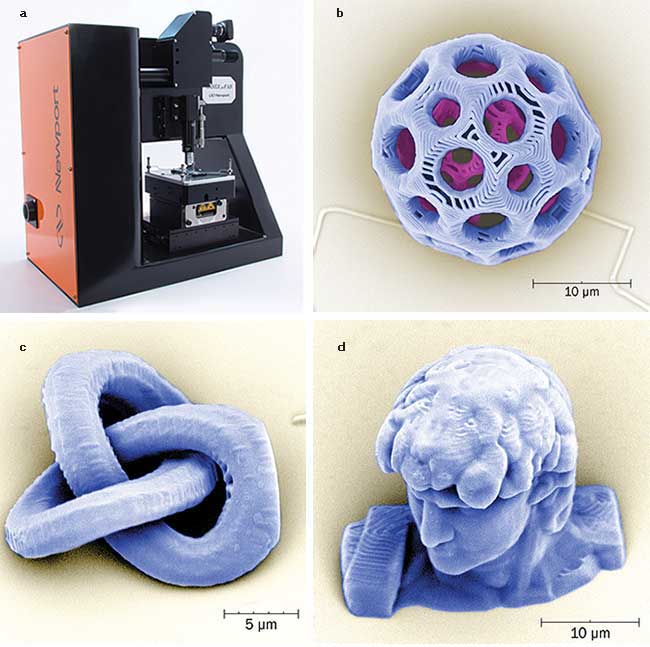
At Newport’s Technology and Applications Center, scientists have developed the Laser μFAB that can be used to fabricated 3D microstructures of unprecedented complexity and with great finesse (Figure 2). A set of high-precision stages are used within the Laser μFAB to move the sample across a fixed laser excitation beam. Although this method of performing TPP allows for patterning large areas that are limited only by the total travel distance of the stages, it also requires the highest performances by the stages. Consequently, the development of such a system involves unique challenges, but solutions are available.

Figure 2. (a) Newport’s Laser μFAB. (b,c,d) False color SEM images of three-dimensional microstructures fabricated by TPP using the Laser μFAB. Courtesy of Newport Corp.
Motion control
The spatial tolerances required by TPP fabrication can be found directly in scanning electron microscope (SEM) images with feature sizes at the submicron scale and tolerances measured in nanometers. While SEM images provide a clear picture of the spatial tolerances, the dynamic tolerances are not always readily transparent. These dynamic demands come in part from the nonlinear nature of the TPP process and are especially evident in the uniformity of periodic structures in 3D lattice arrays and feature sizes near the TPP process limit.
Fabrication of three-dimensional periodic microstructures is especially demanding because the motion system must demonstrate repeatability in six degrees of freedom to the nanometer scale. This puts specific demands on flatness and straightness as well as Abbe error induced from parasitic angular motion, such as pitch and yaw deviations. TPP processes using a high NA microscope objective focused spot are also characteristically slow. This means that the impact of motor heating over extended operating times should be negligible. This also introduces constraints related to in-material focus and the flatness of the stage to hold process planarity and correct optical axis height.
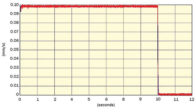
The slow process speeds of TPP, combined with the nonlinear nature of the TPP process itself, contribute an extra set of very strict dynamic demands. Precise dosing requires a uniform process velocity to achieve uniform microstructures. This includes coordinated
motion between stages while operating on multiaxis trajectories.

Figure 3. Dynamic ramp and velocity characteristics of scanning XM stage tuned for the TPP process. Courtesy of Newport Corp.
The in-house materials process and motion experts at Newport work together in the lab to optimize the motion system for the TPP process. The unique combination of multi-mode expertise results in motion systems with optimal process-specific PID (proportional, integral, derivative) tuning, inertia compensation and dynamic motion profiling that compensates for second- and third-order dynamic effects as observed in the process results. This combined expertise is delivered in every motion system involved in laser materials processing.
For TPP, Newport uses XM Series linear motor stages. Machined from an airframe aluminum alloy with high tolerance proprietary machining processes, XM stages are both light and stiff. Capable of submicron flatness/straightness over 50 mm of travel and repeatability of 40 nm over those same dimensions, XM stages excel at performance levels demanded by TPP. Combining a frictionless, direct-drive system with a large center-driven thermally decoupled ironless linear motor and high-resolution direct red encoder, XM Stages achieve <0.1 percent velocity stability, negligible heat impact at the material and general performance characteristics to make uniform, repeatable structures to 100-nm feature sizes.
Beyond motion control
One way to further improve the prospects of TPP manufacturing is with more advanced laser-synchronized motion. A challenge for laser processing is synchronizing the firing of a laser with the motion path. Typical lasers are fired based on an internal clock with very short pulses, so attempting to synchronize this with an external motion signal can lead to missed pulses and substandard results. Newport has developed a unique methodology for synchronizing the triggering of the laser with a multidimensional motion path with less than 100 ns of latency, with up to 12 MHz pulse rates, allowing accurate pulse separation/overlap at the submicron scale while moving at speeds on the order of meters-per-second. The result is optimal throughput with highly accurate and repeatable features.
Microstructured materials are a new frontier in technology with the potential to bring innumerable and unimaginable benefits. This will only be achieved through full-scale commercial TPP manufacturing, and one key to realizing this scale is submicron motion control. Fortunately, the precision motion control industry’s 50 years of research and development are well positioned to meet the challenges.
Meet the authors
Tommaso Baldacchini is a staff scientist with Newport Corp., a subsidiary of MKS Instruments Inc., in Irvine, Calif.; email: [email protected]. Matthew Price is a senior business development manager with Newport Corp.; email: [email protected]. Phong Dinh is a senior applications engineer with Newport Corp.; email: [email protected].
Laser Quality Matters in Additive Manufacturing
KEVIN D. KIRKHAM, OPHIR-SPIRICON LLC
Additive manufacturing and 3D computer-aided design (CAD) have radically altered how prototype, developmental and customized mechanical components are created. Now the landscape is again changing as direct laser melting, selective laser sintering or metal 3D printing quickly become widely used for critical, customizable or hard-to-fabricate constructs.
Additive manufacturing starts as a high-power fiber laser beam is directed onto a table of metal powder. The laser beam then draws the net shape of the component, melting a few tens of microns thickness at a time as the 3D CAD model is transformed into a durable, accurate and reproducible mechanical component.

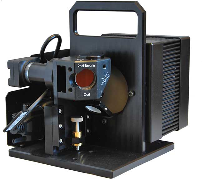
Spiricon’s HP-FSM-PM combines a 600-W power sensor and CCD camera to measure the focused beam at the work surface. Courtesy of Ophir-Spiricon.
Metal powder must be accurately laid across the build area to an exacting thickness while a focused laser beam of known dimension, power and focal spot location is directed to construct the net shape one thin layer at a time. To ensure the metal is completely reflowed — creating the strongest, most homogeneous structure possible without overheating portions of the construct — the power density and location of the focused laser beam must be consistently known.
Data describing how the laser beam focuses to achieve the operational envelope should be analyzed before and after any critical part is made. While laser power and beam profile measurements have become ubiquitous in this age of using lasers for everything from mosquito abatement to personal electronics security systems, measuring the actual beam that interacts with the powder in these systems is anything but straightforward.
To understand the parameters of the process, it is important to know the power density profile of the laser beam. Total power, focused spot size and focal plane location describe the working beam, but these parameters can change as beam delivery optics heat up over time. Numerous measurement systems are deployed to try to track these variables and to attempt to constrain the variations so that consistently accurate constructs may be achieved.
Camera, scanning pinhole and noncontact, Rayleigh scatter-based beam profilers measure the delivered beam. These beam profiling systems can help the AM system user map the beam in space, but a National Institute of Standards and Technology (NIST) traceable power/energy measurement device must also be employed so that the power density profile of the delivered beam can be measured to known standards. Hybrid laser measurement systems that include power or energy measurement, beam profile and beam location sensors are needed. Such systems accurately assess the power density profile of the delivered beam as well as the location and consistency of these parameters.
Hybrid systems that include camera-based beam profiling and a laser power sensor help users of additive manufacturing systems understand the process. The camera is precisely located at the build plane so that an accurate power density model of the working laser beam, at the working plane of the additive manufacturing machine, can be made. These hybrid systems measure focal spots from 37 µm to 2 mm and laser power up to 600 W, providing the user with real-time measurements.
Meet the author
Kevin D. Kirkham is the senior manager of product development with Ophir-Spiricon in North Logan, Utah; email: [email protected]
/Buyers_Guide/MKS_Newport/c10218
/Buyers_Guide/MKS_Ophir_Light_Measurement/c10765
Published: September 2016
Glossary
- two-photon polymerization
- Two-photon polymerization (TPP) is a technique used in additive manufacturing, specifically in the field of 3D printing. It involves using a focused laser to polymerize a photosensitive material in a precise and controlled manner. The process relies on the nonlinear absorption of photons, where two photons are absorbed simultaneously to initiate a chemical reaction that leads to polymerization.
Here is a breakdown of the key components and steps involved:
Photosensitive material: The...
- additive manufacturing
- Additive manufacturing (AM), also known as 3D printing, is a manufacturing process that involves creating three-dimensional objects by adding material layer by layer. This is in contrast to traditional manufacturing methods, which often involve subtracting or forming materials to achieve the desired shape. In additive manufacturing, a digital model of the object is created using computer-aided design (CAD) software, and this digital model is then sliced into thin cross-sectional layers. The...
- polymerization
- Process of synthesizing long molecular chain materials (polymers) by reaction of many small molecules (usually thousands) called monomers.
fiber lasersmultiphoton absorptionpulsed lasersMKSOphir-Spiriconlaser profilingKevin KirkhamTommaso BaldacchiniMatthew PricePhong DinhindustrialLaserstwo-photon polymerizationTPPultrafast lasersMicrostructuresNewportLaser µFABadditive manufacturingpolymerizationFeatures