In the same way that water flows can be manipulated using dams and channels, light can be made to bend by spatially tailoring the material property through which it flows, and transformation optics allows the flow of light to be precisely controlled in desirable ways.
The classical science of light calls on lenses and optical waveguides to collect or distribute the flow of light. But at the nanoscale, the desired behavior and the spatial resolution of the light manipulation become so extreme that standard ray-optics engineering approaches become inadequate. This is where transformation optics steps in.
One of the more headline-grabbing applications of the field is the well-publicized invisibility cloak. This intriguing device works by bending light around itself so as to effectively disappear. But scientific groups are also working on many other valuable applications, including novel optical lenses such as hyperlenses, light concentrators for solar cells and even tiny photonic components for scaling down photonic circuits.
Transformation optics also promises superresolution microscopy, in which sensing of molecules, viruses and DNA is possible with devices that produce subwavelength resolution.
The field is still in its infancy, having drawn the attention of the scientific community in 2006 when the first invisibility cloak was experimentally demonstrated just six months after it was proposed theoretically by professor John Pendry at Imperial College London.
After this, progress was announced quickly and often. In 2008, broadband low-loss optical cloaks were demonstrated by many groups, including professor Xiang Zhang’s at the University of California, Berkeley. More recently, Shuang Zhang’s group at the University of Birmingham in the UK and George Barbastathis’ group at MIT independently reported macroscopic cloaks for visible light without relying on nano- or microfabricated artificial composite materials.

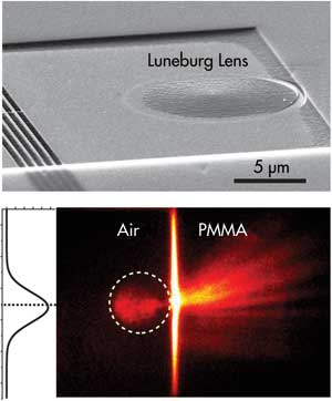
Xiang Zhang’s plasmonic Luneburg lens comprises a polymethylmethacrylate (PMMA) dielectric cone, which can resolve optical waves from multiple directions simultaneously. Courtesy of Xiang Zhang.
Metamaterials and plasmonics
Most of today’s transformation optics relies on metamaterials, artificial metal-dielectric composites with subwavelength features. The quandary facing those working in the field is twofold. First, transformation optics requires fabrication of structures with nonconformal geometries. Second, practical realization of these devices will not be possible with currently available high-loss materials, so improving the constituent materials is essential.
“Purely dielectric (meta)materials are highly desired because of low losses and broadband working wavelengths,” Zhang said. “Semiconductor-based metamaterials could be one good option, since we can combine the advantages of fast and low-loss photonic elements with the superior and highly integrated electronic properties of semiconductor materials.”
Several groups are searching for the best class of material that can lend itself to transformation optics. In one, Paul West and his colleagues in professor Alexandra Boltasseva’s group at Purdue University in West Lafayette, Ind., have been exploring the merits of plasmonic materials, which are beginning to demonstrate their superior performance in optical metamaterials.

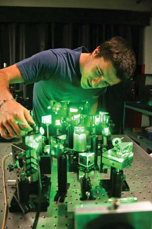
Paul West at Purdue University in West Lafayette, Ind., is exploring the merits of plasmonic materials, which are showing great promise in optical metamaterials. The biggest challenge to overcome in plasmonics is the large loss of energy as a wave travels within such materials. Courtesy of Purdue Nanophotonics Lab.
Plasmonics offers the confinement of micron-size photonics down to the nanometer-length scale. Because plasmonic devices are capable of subwavelength confinement, plasmonics is the fundamental building block for a variety of hot fields in optical research, including metamaterials and transformation optics.
West said that, while plasmonics and its offspring (including transformation optics) show great promise, there are challenges that must be addressed before success in these fields can be realized. “Currently, the biggest obstacle to overcome in plasmonics is the large loss of energy as a wave travels within such materials. This obstacle is quite similar to the material challenges faced in the early days of semiconductor devices.”
The full potential of silicon electronics was not realized until the electronic properties of the constituent semiconductor materials were optimized. Currently, plasmonic devices rely almost exclusively on silver and gold, both of which experience large losses as the frequency of operation increases into the optical range due to interband transitions inherent to the materials.

This image shows silver on a glass microsphere, one example of a structure with nonconformal geometry. A gradient in the filling fraction of materials results in a gradient of effective optical properties. Because of surface energy differences, the silver layer changes from individual islands to a semicontinuous film and, finally, to a continuous film as the filling fraction increases. Courtesy of Purdue Nanophotonics Lab.
“We have experimentally shown that various materials, including transparent conducting oxides and transition metal nitrides, have advantages over conventional plasmonic materials (silver and gold) used for transformation optics devices at certain frequency ranges,” West said. “One of the most important conclusions we have drawn from this work is that no single material will be used for all the various transformation optics devices; rather, a variety of materials will be used in different applications at different frequencies.”
Bending light by design
There are two key approaches to harnessing the flow of light: semiclassical transformation optics and full-wave transformation optics. With the former, a distribution of refractive indices is designed to force light rays to propagate along curved lines, for example. Full-wave transformation optics is built on the invariance of Maxwell’s equations with respect to coordinate transformations and produces the most comprehensive and extreme control of electromagnetic energy flow.
In a paper published earlier this year in Physics-Uspekhi, Dr. Alexander Kildishev and professor Vladimir Shalaev at Purdue University outline both the semiclassical transformation optics and full-wave transformation optics approaches and introduce a variation on light concentrators. They present omnidirectional light absorbers or optical black holes based on semiclassical transformation optics proposed earlier by professor Evgenii Narimanov and Kildishev.
The optical black hole can collect light from all directions, including light scattered from the urban or natural environment, which makes the proposed device ideal for harvesting light for mobile photovoltaic systems. It could also be critical in mobile or stationary low-power-supply systems and, more than ever, in independent “drop and forget” unattended sensing and communications applications.
While metals work well for low incident light frequencies, they begin to suffer from high interband transition losses as the incident light approaches the telecommunications and visible frequencies. Currently, the most common solution to the problem of losses is to use gain media as host materials, so that losses inherent in the plasmonic structures can be compensated by the gain in the host.
Kildishev explains that one advantage of a black hole based on transformation optics is that it can be realized in a purely dielectric design, without resorting to metal elements with their inherent losses.
The next big advances in the field could be discovered thanks to recent interest in harnessing surface plasmon polaritons. While the idea that energy can be transferred from a gain material to surface plasmon polaritons or to plasmons in metal nanostructures using stimulated emission is not new, the first experimental results are promising.
These include the demonstration in 2009 of the world’s smallest laser, accomplished through a collaborative effort between Dr. Mikhail Noginov at Norfolk State University in Virginia, co-authored by Vladimir Shalaev of Purdue University and Ulrich Wiesner of Cornell University in Ithaca, N.Y.
The tiny surface plasmon laser – dubbed “spaser” – combines dye molecules and gold nanoparticles within a silica shell floating in water to generate enough energy to produce surface plasmon oscillations. The resulting laser light is emitted at a wavelength of 531 nm, which makes the device the smallest laser operating in the visible.
UC Berkeley’s Zhang has so far demonstrated a plasmonic Luneburg lens to focus surface plasmon waves and a plasmonic Eaton lens to bend surface plasmon waves, as well as various photonic elements with multiple functionalities, which are useful for further scaling down the size of integrated photonic circuits.
A remarkable achievement made by Kildishev and his colleagues at Purdue is the experimental demonstration of a low-loss active negative-index metamaterial, reported in a paper published in Nature in 2010. In the setup, the team incorporated a fluorescent dye into the metamaterial layer to minimize the amount of light that is absorbed.
This principle could be expanded if the team were to replace the dye with a semiconductor material that can be pumped using an electrical, rather than an optical, signal. This variation would be easier to integrate with conventional optoelectronics.
With myriad optical applications, it is easy to overlook the many other areas in which the premise of transformation optics could be applied. For example, Zhang suggests that future breakthroughs may not be limited to electromagnetic waves.
“The principle of transformation optics can be applied to other waves, such as acoustic waves, matter waves, etc.,” he said. “In my opinion, manipulating the electron matter waves for electronic devices could be very interesting.”