Xing-Fei He and Nixon O, Teledyne Dalsa Inc.
Using a sensor architecture that permits photoelectrons generated from multiple exposures to be summed with no additive noise enables high-speed imaging under light-starved conditions. This technology has become a standard in the automated inspection of flat panel displays and is expanding to markets such as photovoltaic panel inspection.
Time delay integration (TDI) imaging technology enables high-speed in-line automatic optical inspection (AOI) of high-performance displays such as those used in iPhones, iPads and high-definition televisions. The $130 billion flat panel display industry relies on TDI technology to ensure that every picture is perfect.
Recently, low-temperature polysilicon used for in-plane switching liquid crystal displays and organic LEDs has pushed pixels to very small dimensions. For example, the iPhone's Retina display has a density of 326 pixels per inch and a subpixel size of about 26 µm. The increasing density results in a demand for higher-speed and higher-resolution digital imagers that become increasingly light-starved and, in turn, need even higher responsivity. TDI technology is a proven solution that can meet these often conflicting demands.
New TDI products are increasingly capable of imaging beyond the visible range. The finer display structures have led to the use of light sources with shorter wavelengths down to the ultraviolet.
Concurrently, the solar panel industry is becoming more automated as it boosts production capacity. In-line inspection of silicon solar cells has low-illumination requirements, similar to those of flat panel display inspection. However, solar cells emit electroluminescent or photoluminescent photons with wavelengths around 1150 nm. Hence, solar cell inspection requires cameras that can detect near-IR photons.
Line-scan and TDI technologies
Line-scan cameras operate differently from area-scan cameras. With an area-scan camera, a matrix of pixels provides an image of the object, which contains both length and width information within a single image. Line-scan cameras capture images one line at a time as the object being imaged moves past the field of view. A series of pictures is taken continuously, with the pixel capture rate timed to be in sync with the speed of the moving objects (Figure 1). This series of one-dimensional images forms a long two-dimensional image.
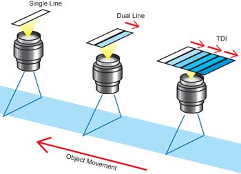
Figure 1. Various line-scan technologies: single-line, dual-line and time delay integration (TDI). To achieve high responsivity, TDI uses multiple stages to capture multiple exposures. In these stages, photogenerated signal charges are transferred in sync with object motion. Dual-line scans are considered two-stage TDIs.
The advantage of line-scan imaging is that it can image at very high speeds — as in hundreds of thousands of lines per second. With an area-scan camera, the system must wait for the camera to transfer the entire multimegapixel image data out of the sensor before the camera can capture another image. With a line-scan camera, only a single line of data must be transferred out before the next exposure. This approach allows a line-scan camera to produce continuous images as wide as the sensor but of virtually unlimited length. Increasing imaging speed requires brighter illumination. The reality is that AOI often ends up in a light-starved situation, either because the light source is not bright enough or safety is a concern.
CCD TDI is a special type of line-scan technology based on multiple exposures of the same moving object to achieve higher responsivity.1 In TDI operation, the speed at which a charge packet containing image data is transferred within the CCD is in sync with the speed of the moving object, allowing the data packet to track the motion of the object. Photogenerated electrons are transferred from one TDI stage to another in the charge domain. The transfer is accomplished without adding any noise. Because the detector signal is proportional to the number of stages, the signal-to-noise ratio scales linearly with the number of stages. With resolutions of up to 12,288 pixels, a 5.2-µm pixel size, 512 TDI stages and a maximum line rate of 90 kHz, Teledyne Dalsa's Piranha HS TDI camera family provides responsivity of more than 1000 (8-bit DN [digital numbers])/(nJ/cm2) at minimum camera gain.
Figure 2 plots the responsivity results of various standard line-scan and TDI cameras as a function of the inverse of the maximum line rate. The output signal of an imager is proportional to the product of the responsivity and the exposure time, for a constant light intensity. As a result, applications with a higher line rate will require cameras with higher responsivity capabilities to maintain a useful signal-to-noise ratio. CCD TDI clearly outperforms single-, dual- and quad-line-scan technologies because it can incorporate hundreds of stages in the detector. Although TDI does not have exposure control, pulsed LED lighting can be used to maintain a constant exposure time when the object motion speed varies.
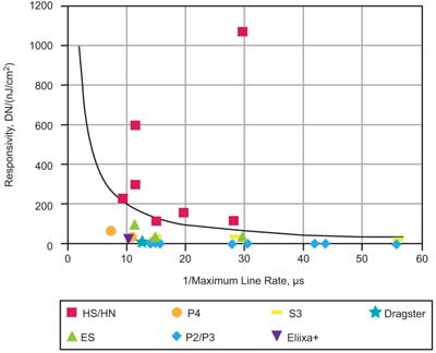
Figure 2. Responsivity (at minimum gain, 8 bits) versus the inverse of the maximum line rate of various line-scan cameras. HS and ES from Teledyne Dalsa are CCD TDI cameras. The Eliixa+2 from e2v Ltd. is a CMOS quad-line scan. P4 from Teledyne Dalsa and Dragster3 from Awaiba are CMOS dual-line scans. P2 and P3 from Teledyne Dalsa are CCD single-line scans. The solid line plots the responsivity required to achieve a 200-DN (digital number) signal with an irradiance level of 100 µW/cm2.
Signal-to-noise ratio
In many imaging applications, two types of noise are most important. The first, called read noise, is associated with "reading" the signal — that is, converting photogenerated signal charges into a voltage and then to a digital output. The second, photon shot noise, is associated with quantization of the incident illumination into a finite number of discrete photons. Other sources of noise exist, but they are much less important than the above.
In CCDs, the read noise (σR) is fixed because photoelectron signal packets are converted only once, after they have been transferred to a readout structure at the edge of the CCD array. In CCD TDIs, the read noise remains fixed regardless of the number of stages. In CMOS, because charges must be read before the signal can be transferred out of each pixel, each read results in its own noise. Consequently, a dual-line-scan CMOS array will have √2x the read noise of an equivalent single-line-scan CMOS array. Similarly, an n-stage CMOS TDI array will have √nx the read noise of an equivalent single-line CMOS array.
The photon shot noise (σPS) is always equal to the square root of the number of photoelectrons collected and read (S), except in highly unusual situations, such as in the deep-UV when each photon can generate multiple photoelectrons. Because the ratio of the signal S to the photon noise (σPS) is always equal to √S, it is always advantageous to increase S to maximize the signal-to-noise ratio. TDIs can increase S without increasing the incident illumination.
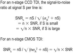
In light-starved conditions where the signal S is small, CCD TDIs achieve the best signal-to-noise ratio.
Automated display inspection
A thin-film transistor (TFT) LCD is a sandwich of two panels with liquid crystal material in between. An array of transistors on the TFT panel controls the polarization of the liquid crystal and, hence, the light intensity. Another panel contains an array that filters out the spectra of each primary color (red, green and blue) for each subpixel.
A high-definition television (1920 x 1080 pixels) screen has about 6 million subpixels. The industry adopts a zero-defect policy; thus, every subpixel must be perfect.
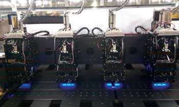
Figure 3a. This automatic optical inspection system for thin-film transistor (TFT) arrays uses Teledyne Dalsa's HS-12k/5.2-µm 256-stage TDI cameras. Light sources are selectable red, green, blue or white LEDs. Courtesy of Favite Inc.
The AOI systems for flat panel displays must operate in-line with the production flow. This helps minimize handling of the large, thin glass panel blanks (0.3 to 0.5 mm thick) to avoid breakage. They also must be fast enough to avoid becoming a bottleneck in the production flow. In a $3 billion fab, takt time is a key metric to ensure that the production throughput will meet the expected return on investment. To prevent the inspection system from limiting production flow and increasing the takt time, high-speed cameras are required.
Automatic optical inspection for TFT arrays is one of the most challenging applications today, and all array AOI systems use CCD TDI cameras. Speed and resolution are increasing with the adoption of low-temperature polysilicon in smartphones, where the pixel size is smaller than the pixel size in amorphous silicon panels used in televisions. The TFT pixel is only a few microns across. This requires an AOI object resolution of about 1 µm, and it is getting even smaller. This is close to the spatial resolution limit of most optical systems.

Figure 3b. Images of TFT structures with different lighting conditions: (a) viewed under a microscope; (b) front illumination; (c) backlight; and (d) both front illumination and backlight.
Figure 3a is an advanced TFT array AOI system developed by Favite Inc. of Hsinchu, Taiwan. At the core of the system are Teledyne Dalsa's latest HS-12k/5.2-µm 256-stage TDI cameras. The system can accommodate G8.5 glasses (2500 x 2250 mm) and can detect defects in TFTs with an object resolution of 0.8 to approximately 2 µm (see Figure 3b). Multiple scans are performed at a line rate of 80 to approximately 90 kHz to cover the entire glass. The number of TDI cameras in the system depends on the end user's requirements. Because some areas (e.g., pixel area) are transparent while some (e.g., metal pad) are opaque, both front and back illuminations are used with selectable red, green, blue or white light sources. Figure 3b shows that simultaneous front and back illumination produces images with the contrast necessary to detect many types of small defects.
Beyond the visible spectrum
Color filters also require in-line high-speed automated inspection. Figure 4 shows an advanced AOI system for color filters developed by Utechzone Co. Ltd. of Taipei, Taiwan. The system uses Teledyne Dalsa's ES-8k/7-µm 32-stage TDI cameras. In its single-pass design, 34 cameras are installed in two separate lines. Seventeen cameras capture images with angled front illumination, while the remainder capture backlit images. The system inspects G8.5 glasses at 450 mm/s with a resolution of 8 µm.
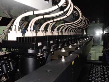
Figure 4. This automatic optical inspection system for color filters uses Teledyne Dalsa's ES-8k/7-µm 32-stage TDI cameras. The single-pass system uses 34 cameras. Courtesy of Utechzone Co. Ltd.
As a de facto standard for the flat panel display AOI industry, the Piranha HS TDI camera continues to evolve to meet future requirements. The next generation features even higher spatial resolution and lower noise. Backside thinning and thick detection layers are a few of the technologies that Teledyne Dalsa has developed. The quantum efficiency at different wavelength ranges can be optimized for UV, visible or near-IR imaging.
The HN-8k/7-µm 256-stage TDI is a new camera for near-IR imaging. At the minimum gain setting, it has a broadband responsivity of 1078 (8-bit DN)/(nJ/cm2); at the 1-µm wavelength, its responsivity is 420 (8-bit DN)/(nJ/cm2). Figure 5 compares the quantum efficiency spectra of the HS-8k/7-µm and HN-8k/7-µm TDI cameras. Unlike the HS TDI camera, which has vertical anti-blooming structures that reduce near-IR response, the HN TDI has lateral anti-blooming, resulting in enhanced sensitivity in the near-IR.
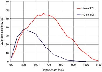
Figure 5. The quantum efficiency of HS and HN TDI cameras: HS TDI is designed for visible imaging, while HN TDI is optimized for near-IR imaging applications.
Solar panel manufacturing continues to adopt automation, and AOI plays a key role. Currently, wafers are inspected at a speed of about one per second. The normally poor CCD sensitivity in the near-IR is the limitation for electroluminescence and photoluminescence imaging techniques that are particularly effective in revealing microcracks that can occur during the processing.
To detect electroluminescent and photoluminescent signals, the HN-8k TDI camera provides responsivity comparable to that of InGaAs cameras at ~1 µm. Compared with InGaAs imager-based systems, however, the HN-8k has a much lower system cost. Because of this, TDI imaging is becoming an enabler in automating high-volume solar panel manufacturing.
Meet the authors
Dr. Xing-Fei He is senior product manager at Teledyne Dalsa Inc. in Waterloo, Ontario, Canada; email: [email protected]. Dr. Nixon O is technical director at Teledyne Dalsa; email: [email protected].
References
1. S.G. Chamberlain and W.D. Washkurak (July 1, 1990). High-speed, low-noise, fine-resolution TDI CCD imagers. Proc SPIE, Vol. 1242, pp. 252-262.
2. e2v Ltd. Eliixa+ 16k pixels CMOS line-scan camera datasheet: http://tinyurl.com/7ju9z5z.
3. Awaiba Dragster linescan sensor short spec sheet: http://tinyurl.com/7952784.