Wafers yield thermal benefits in photonic devices.
Hank Hogan
Besides being a girl’s best friend, diamonds could be a pretty good pal of ultrabright LEDs and laser diodes — provided a new material from Group4 Labs LLC of Menlo Park, Calif., is used successfully in products. The company has devised a way to deposit a thin layer of GaN on polycrystalline diamond. Because diamond is a very good conductor of heat, devices built in the GaN would run cooler and, therefore, better.
This benefit applies to transistors and, especially, to lasers and LEDs, Group4’s CEO Felix Ejeckam said. In emitters, he explained, negatively charged electrons and positively charged holes can be consumed in producing photons or phonons, lattice vibrations that conduct heat.
“Every electron-hole pair that goes into creating phonons is a pair that isn’t going into creating photons,” Ejeckam said. “Phonons also trigger more phonons.”

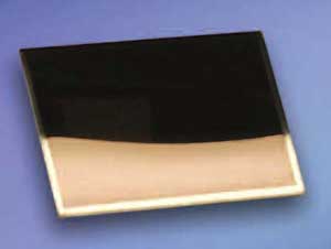
The new substrate material, initially available in 10 × 10-mm wafers, features a layer of GaN on polycrystalline diamond. Courtesy of Group4 Labs LLC.
Depending on its quality, manmade diamond has a thermal conductivity of more than 1200 W/m.K. That compares with 350 W/m.K for SiC, 150 W/m.K for silicon and 40 W/m.K for GaN.
In the new material, a freestanding 25-µm-thick layer of diamond is capped by a 750-nm-thick layer of GaN. Heat generated by a device in the GaN is rapidly carried away. According to simulations, a 100W/cm transistor built on a GaN-on-diamond wafer would be at least 240 °C cooler than one on a conventional substrate.
Making this material takes a bit of technical wizardry. For one thing, the crystal mismatch between diamond and GaN can lead to GaN dislocations and defects. Another problem is a difference in the coefficient of thermal expansion that can lead to problems as the temperature varies with device operation.
Ejeckam would not reveal his company’s techniques for accomplishing this marriage of materials, but he does claim success.
“We’ve been able to make very good bonds between the GaN and the diamond,” he said. “We’ve tested those bonds, and we’re very happy to send samples out to people who want to do further tests.”
Group4 plans to supply the material for others to use in making products. Ejeckam said that the optical market for GaN-on-diamond wafers probably will involve applications that need bright sources. He added that a series of announcements for additional products and materials are planned this year.