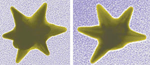
They can be in the form of rods or rice, cups or cubes, spheres, stars – even shells. No, they’re not new marshmallow shapes for kids’ cereal, they’re nanoparticles, incredibly small structures said to have powerful potential in solar cells and cancer treatments.
The 1985 discovery of carbon atoms bound in the form of a ball – fullerenes – by Richard E. Smalley, Robert F. Curl Jr. and Sir Harold Kroto (the trio received the 1996 Nobel Prize in chemistry) coupled with the invention of more powerful microscopes, set the stage for advances in nanotechnology – working with particles on the scale of atoms and molecules.
The scanning tunneling microscope, developed in the early 1980s, provided 3-D images of atomic-level objects for the first time. The atomic force microscope, created in the mid-1980s, uses a sharp probe to magnify the surface features of an object in three dimensions.
Once researchers could observe materials on those scales, they soon discovered that the physical properties of materials can change because of quantum confinement effects. That led to new understandings of plasmonics, a field of optics that aims to develop new optical components and systems the size of today’s tiniest electronic chips but with the speed of photons, which could prove useful for applications including biological sensing, microelectronics, chemical detection and drug delivery.
Plasmons are created when light hits the surface of a metallic nanostructure at a particular angle, causing waves to propagate through electrons near the surface.
In 2003, researchers at Rice University in Houston discovered that the type of plasmon that exists on a surface is directly related to its geometric structure, and that, when the light striking a plasmon oscillates at the same frequency, the plasmon harvests the light and converts it to electrical energy, which propagates through the nanostructure and is eventually reconverted to light.
The work helped shift much of the emphasis away from simply altering the size of nanoparticles and toward creating more intricately shaped ones to discover how the shapes themselves affect light interaction.
In 1998, Naomi J. Halas, the Stanley C. Moore professor of electrical and computer engineering and a professor of chemistry at Rice University, invented metal spheres called nanoshells. These glass cores, covered by thin gold shells – think microscopic malted milk balls – are about 20 times smaller than a red blood cell, making them perfectly sized for interactions in biological systems.
By controlling the size of the nanoshells and the ratio of the core to the shell, Halas and her team control the wavelength of light that the nanoshells will absorb. Once they absorb the light, they can generate heat. Because the particles are benign, they are being pursued as a nontoxic way to target cancer treatment to specific solid tumors, such as in cancers of the head, neck and breast.
The nanoshell patents have been licensed to Nanospectra Biosciences Inc., a company founded by Halas’ Rice colleagues and commercialized under the name AuroLase Therapy. The AuroShell particles are administered intravenously, traveling through the bloodstream and entering the tumor through its weakened, leaky capillaries. Once in place, the nanoparticles are heated via infrared laser light supplied by a fiber optic probe inserted in or near the tumor. The excess heat ablates the tumor with minimal damage to surrounding healthy tissue. The company concluded animal testing in 2007 and is currently conducting a pilot study for head and neck cancer in humans.
In 2006, engineers, physicists and chemists at Rice University’s Laboratory for Photonics (LANP), under the direction of Halas, announced the invention of nanostars, nanorice and nanoeggs.
A star is born
Nanostars, virus-size, spiky-surfaced gold particles, have the potential to become powerful chemical sensors because they deliver strong spectral peaks that are easy to distinguish with relatively low-cost detectors.
The LANP researchers found that each spike on a nanostar has a unique spectral signature that could be used to discern the orientation of the nanostar in three dimensions, opening up new possibilities for 3-D molecular sensing.
Recent work by bioengineers at Duke University in Durham, N.C., indicates that star-shaped gold nanoparticles may be better than all others for certain applications. Because nanostars can enhance reflected light much better than other shapes of nanoparticles, they have more potential as traces, labels and contrast agents. They also are thought to have the ability to be “tuned” to identify particular molecules or chemicals.
The Duke researchers used nanostars in conjunction with surface-enhanced Raman scattering (SERS) for chemical and biomedical detection.
“This study is the first demonstration that these nanostars can enhance the effect of SERS to produce strong and unique signatures, like ‘optical fingerprints,’” said Tuan Vo-Dinh, director of the Fitzpatrick Institute for Photonics at Duke, in a university publication.
Scientists at the National Institute of Standards and Technology (NIST) employed SERS to test the optical qualities of silver and gold nanostars, using two target molecules in solution. They reported their results last fall in the Journal of Raman Spectroscopy.

NIST scientists found that gold and silver nanostars improve the sensitivity of surface-enhanced Raman spectroscopy (SERS) by 10 to 100,000 times over other commonly used nanoparticles. The stars may be used one day in applications including disease diagnostics and contraband identification. Courtesy of NIST.
NIST physicist Angela R. Hight Walker and her team found that the Raman signals of the molecules (2-mercaptopyridine and crystal violet) were 10 to 100,000 times stronger when nanostars were used instead of other nanoshapes, such as rods or spheres.
Hight Walker and her team built their gold nanostars from the bottom up, using surface alterations to manipulate their growth and control their shape. Once the nanostars were suspended in the solution, the researchers guided them to gather together in “hot spots” of larger Raman enhancement.
Rice and eggs, please
In March 2006, Rice University announced that Halas’ group had created nanoparticles of gold and iron oxide that resemble grains of rice. Nanorice combines the best properties of spheres and rods – two of the most optically useful shapes – to focus light on a small area.
As with nanoshells, nanorice have a nonconducting metal core covered by a gold shell, but nanorice were found to have a greater ability than nanoshells or nanorods to change the shape of a metal at the nanoscale. Nanorice also were found to be more sensitive surface plasmon resonance nanosensors.
Halas’ group unveiled the “nanoegg” in August 2006. Nanoeggs are about the same size as nanoshells but interact with five times the number of light wavelengths because of their asymmetric structure, which allows them to focus more energy on a particular spot.
Nanocups runneth over
In a February 2009 issue of the journal Nano Letters, Halas and a member of her group, graduate student Nikolay Mirin, explained how they created a cup-shaped material that can collect light from any direction and emit it in a single direction. The light-bending metamaterial is being investigated for applications in high-powered optics, ultraefficient solar cells and even cloaking devices.
The tiny cups essentially were material left over after the punching of nanosize holes in a thin gold film. Once Mirin devised a method of preserving the cups’ orientation, the researchers discovered their proficiency for redirecting scattered light. They now are working to implement nanocups into a useful device.
Nanoparticles leading the way to light-driven computers
by Lynn M. Savage, Features Editor, [email protected]
Great efforts are under way to maintain the momentum of Moore’s law, increasing the amount of available computing power by continually shrinking circuit board features from transistors to pixels. However, it is increasingly difficult and expensive to find ways to slice and dice the materials used for chip electronics. Furthermore, even if computer chip production were easy and cheap, feature size ultimately would hit the wall of an absolute minimum, and the increased need for power to run these elements would drive up cooling requirements because excess heat is dangerous and eliminates efficiency gains.
For several years now, however, another effort has been under way – spread out among many different academic and commercial labs – that aims to advance the state of the art in computing by planting it in the realm of photonics. Optical computing – using photons instead of electrons to transmit data – has several fundamental advantages: It is much faster, doesn’t generate as much heat and provides much higher bandwidth.
As do their electronic ancestors, photonic computers require couplings between parts. With electronics, such couplings can be as simple as solder and wire – materials that readily permit the flow of electrons between transistors on a chip or between data cables and circuit boards. To couple light-driven transistors, you must be able to guide photons down perfectly shaped pathways; otherwise, the light will reflect out of the device, carrying your data with it. Furthermore, you must be able to confine light tightly enough to compete with the integration density electronic VLSI can achieve.
Confining light and taking it where you need it is traditionally done with fiber optic lines or dielectric waveguides, which work by allowing light to travel down a central core while outer layers keep most of the light from escaping. These conventional waveguiding methods, though, are subject to the diffraction limit in terms of how tightly light can be confined.
Making sure that the light is transmitted by a waveguide without spilling over to an adjacent optical element less than a wavelength away is a major sticking point to the further development of optical computers.
According to Lih Y. Lin, an associate professor at the University of Washington in Seattle, the key to efficiently coupling parts of a photonic circuit with high integration density is sub-diffraction-limit waveguides, and one solution may be the quantum dot.

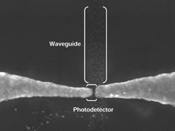
Quantum dots (QDs) can be used to form a waveguide that channels laser light through photonic circuitry. In this scanning electron micrograph, a 52-nm-wide QD waveguide is seen integrated with a photodetector that has a 12-nm gap. The detector is composed of the same QDs as the waveguide. Courtesy of the Journal of Nanophotonics.
Quantum dots – essentially artificial atoms made of semiconductor materials such as cadmium selenide – are well recognized for their use as fluorescent markers in medical imaging and similar applications. The size of the particles controls what color light they emit after they have been irradiated by laser light, and they are highly efficient emitters of light once they get going.
Lin’s group has found a way to take advantage of the nanometer-scale particles’ attributes and turn them into waveguides, confining incoming light in spaces smaller than the wavelength of the light itself and passing it along to the next stage of the computer chip.
There are other ways to guide light in tiny circuits, including using laser light to excite plasmonic materials. “Quantum dots aren’t as prone to transmission loss as other possible subdiffraction-limit techniques,” Lin said. “Some other techniques are still hindered by the diffraction limit.”
The quantum dots can be placed onto a photonic circuit by a number of methods, including deposition or by combining them with other molecules that will guide the nanoparticles into self-assembled patterns. Once energized by a laser beam that is pulsing to deliver binary data, the quantum dots will channel the light throughout the chip in what Lin calls “a cascade of stimulated-emitted light.” Testing the output of experimental systems requires the use of photodetectors now; in the future, output will go to photonic transistors, logic gates and beyond.
“Applications for photonics devices can be driven by the first optical transistors,” Lin said.