The technology for fabricating computer-generated holograms is demanding and requires advanced lithographic techniques.
Uwe D. Zeitner, Fraunhofer IOF; Michael Banasch, Vistec Electron Beam GmbH; and Ernst-Bernhard Kley, Institute of Applied Physics, Friedrich Schiller Universität
Computer-generated holograms (CGHs) play an important role in the modern optics used for generating application-specific optical fields and functions. Their ability to transform incident beams into wavefronts is based upon micro- and nanosize surface structure data that is calculated by computer. Typical applications include interferometric testing of high-precision aspheric lenses, splitting an illumination beam into a number of equal-intensity spots and highly efficient coupling of laser light into optical fibers.
The fabrication of CGHs is based on lithographic technologies, such as laser or electron beam (e-beam) lithography, combined with reactive ion etching for pattern transfer from the resist layer onto the substrate. Modern lithography equipment can expose large substrates to the required diffractive optical pattern with high resolution and accurate placement. The latter is the key to achieving a precise diffracted optical wavefront from the CGH. The fabrication of CGHs requires an extremely demanding technology for the precise generation of the microstructures. Such a platform, dedicated to modern high-end microstructuring techniques for optical applications, has been installed at Fraunhofer IOF in the Center for Advanced Micro- and Nano-Optics (CMN-Optics).
Lithographic process chain
The quality of CGHs is influenced by the substrate and by the lithographic generation of the resist pattern and its transfer onto the fused silica by a dry-etching process. For high-end CGHs, special substrates are required with flatness below 0.5 μm across the patterned area. Because these substrates are nonstandard, they were routinely available, but for e-beam lithography, they required special preparation such as chromium or resist coating. Sputtering of the chromium layer and coating with resist are done in-house with CMN optics. The cleanroom for the resist process is amine filtered so that chemically amplified modern resists can be used. The whole process chain can handle substrates up to 230 × 230 mm (mask blanks) and circular wafers as large as 300 mm.
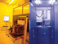
E-beam writing is at the core of the process chain. The special requirements for this step include positioning optimization and accuracy of critical structure dimensions, along with high throughput and stability over exposure times of up to several days. For this task, the SB350 OS (Vistec) e-beam tool is suitable (Figure 1). The abbreviation OS, or “optics special,” indicates high-speed grating writing in cell projection mode and flexible use of substrates. In optical applications, the instrument can handle substrates as thick as 15 mm in sizes as large as 310 × 100 mm, besides standard-size masks (230 mm and 6, 5, 4 and 3 in.) and wafers (150 mm and 4 and 3 in.; also 200 and 300 mm).

Figure 1. This electron beam writer, SB350 OS, has been adapted to the needs of optical structure fabrication.
The writing strategy is optimized for high throughput with variable-shaped beam (maximum shape size 2.5 μm), vector scan and write-on-the-fly modes. The tool is prepared for the software “flexible stage speed,” which adapts the writing rates to local pattern density so that exposure times for large CGHs can be reduced by up to 40 percent. For transferring the pattern onto the large fused silica substrates, two reactive ion etching tools of type SI-500-300 (Sentech) are available. Although the optimization process for these machines has not been completed, the final homogeneity of the etching depth is expected to be better than 3 percent over 230 mm, which would satisfy the tight tolerances of high-end CGHs.
Highest wavefront precision
As noted, the positioning accuracy of the lithographic writing process directly influences the wavefront accuracy of the final optical function. The positioning accuracy itself depends upon the writing speed: the longer the writing time, the stronger the potential influence of drift effects or other external disturbances. For large-size elements, the variable-shaped beam- and cell-projection writing strategies allow a relatively fast exposure. For example, the cell-projection mode allows gratings with periods of 200 nm, 500 nm or 1 μm to be exposed with a writing speed of up to 140 mm2/min.

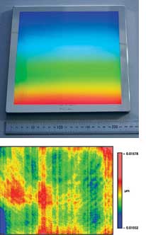
Figure 2. Shown is a large binary grating of 1-μm period and measured wavefront map (size of measurement area: 103 × 80 mm). The positioning error caused by the lithography process is less than 3 nm root mean square.
Writing strategies and the ability to realize such structures on thick substrates open the way for fabricating elements of highest wavefront accuracy. Figure 2 shows such a 1-μm period grating with an extension of 200 × 200 mm, along with an interferometric wavefront measurement of the first diffraction order. Measurement was achieved by placing the grating in a Littrow arrangement in front of a plane wave interferometer. This configuration is characterized by tilting the grating with respect to the incident beam until the first diffraction order is reflected exactly in the direction of the illumination and, in our measurement setup, directly back into the interferometer. Inaccuracies of the grating line positions will be seen in the interferogram as deviations from an ideal plane wave.
For characterization of lithographically caused positioning accuracy, the planarity of the substrate is of no concern. To eliminate the substrate’s influence from the measurement results, two measurements of the same grating position – but with opposite grating tilts – were subtracted to obtain the displayed wavefront. The root mean square wavefront error is 2.7 nm. Because of the subtraction of the two measurements, this value represents twice the positioning error of the writing process. Together with the grating period, this positioning error can be calculated from the measured wavefront to be 2.2 nm – a value suitable for the highest demands of various applications.
To make this potential available for CGH fabrication, a number of developments in the entire technology chain are currently under investigation at Fraunhofer IOF. Hot topics include innovative approaches to the generation of exposure data and completely new substrate concepts that achieve the desired optical function right from the beginning.
Meet the authors
Uwe D. Zeitner is manager of CMN-Optics, Fraunhofer-Institut für Angewandte Optik und Feinmechanik (IOF) in Jena, Germany; e-mail: [email protected].
Michael Banasch is an applications engineer at Vistec Electron Beam GmbH in Jena; e-mail: [email protected].
Ernst-Bernhard Kley is head of Microstructure Technology & Micro-Optics IAP at Friedrich Schiller Universität Jena Institut für Angewandte Physik in Jena; e-mail: [email protected].
aCGH Applications: Where Accuracy Is Essential
In micro-optical structures, a high degree of accuracy is essential in a number of applications, such as CGHs for interferometric testing and for improving aspheric optical surfaces. Testing spherical surfaces is straightforward, but testing aspheric surfaces with sufficient accuracy is very demanding.
Typically, the surface under test is used as a mirror in an interferometric setup in which the wavefront of the measurement beam is adapted to the curvature of the test surface by well-corrected lens systems. As long as the test surface is spherical in shape and its center of curvature coincides with the focus of the interferometer lens, the reflected beam has the same spherical wavefront as the illumination wave.
Thus, after a second transition through the interferometer lens, the test beam ideally should be collimated again. Deviations from a spherical profile of the test substrate will be seen in the interferometer signal as wavefront errors.
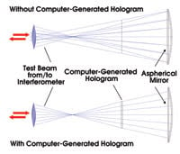
It is obvious that this does not work so easily with aspheric test surfaces because the curvature of the illumination wave basically differs from its shape. As a result, the interferogram obtained by illuminating an aspheric surface with a spherical wave will show a huge number of fringes, and the analysis will become difficult, if not impossible. This situation is sketched in the upper part of Figure 1.

Figure 1. Demonstrated is the principle of interferometric testing of aspheric mirrors with and without CGH.
Overcoming the problem
A CGH is a powerful tool for overcoming this problem. Properly designed and fabricated, such a diffractive element can be introduced into the measurement arm of the interferometer between the interferometer lens and the test surface. The CGH reshapes the incident spherical wave in such a way that the retroreflection condition is satisfied at all points of the aspheric surface under test.
This setup is shown in the lower part of Figure 1. To obtain suitable measurement conditions, a number of critical parameters must be examined. First of all, it is essential that the CGH be well-positioned on the X-, Y-, Z-, ϑ- and φ-coordinates with respect to the incident beam. To assist this positioning, additional diffractive adjustment structures are added to the CGH. These structures directly reflect and diffract the incident spherical wave, and this particular part of the beam can be observed on an interferogram as well.
Furthermore, the position of the test surface with respect to the CGH also must be optimal, and the nonplanarity of the CGH substrate must not introduce additional wavefront errors. Of course, the positioning accuracy of the diffractive pattern contributes to the measurement result. If all potential sources of measurement errors are minimized, the shape of aspheric surfaces can be characterized with an accuracy of λ/10 up to λ/100 or, in extreme cases, even better.

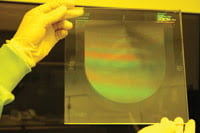
Figure 2. A computer-generated hologram is shown on a 230 × 230-mm mask blank substrate for characterization of a space telescope mirror.
Testing large optical elements can require the use of large-size CGHs. This is especially the case when characterizing large convex telescope mirrors. Figure 2, which pictures a CGH on a 230 × 230-mm substrate, shows an example of such a test. In the near future, it will be possible to fabricate these elements in larger sizes on substrates with an extension up to 300 mm. For this purpose, the technological instrumentation in the field of plasma etching is being updated. This improvement is an essential step to ensure that the high structure precision of about 10 nm obtained in the lithographic exposure step also is retained after pattern transfer into the fused silica substrate with sufficient homogeneity across the large substrate dimension.