Next-generation materials and new computational and fabrication techniques are reshaping how we think about optics.

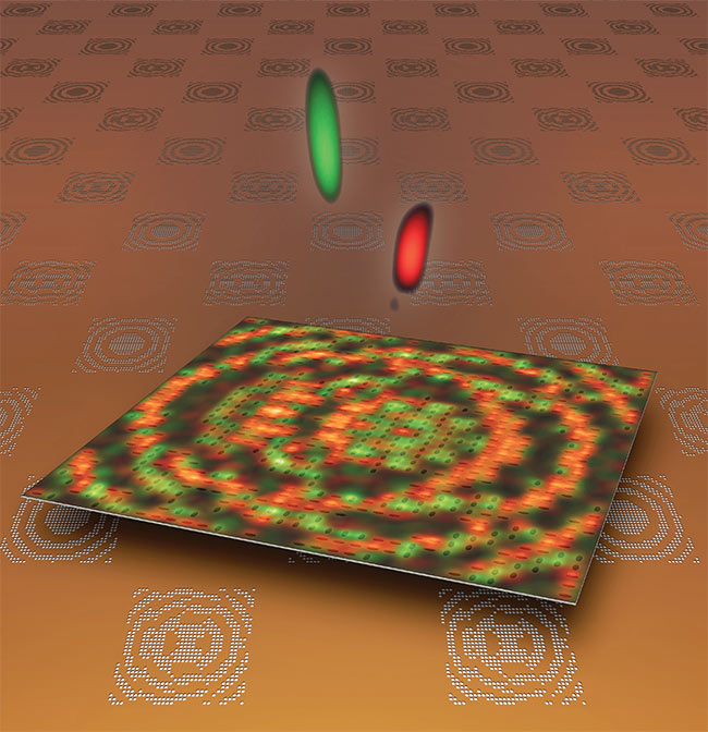
An evolutionary computational algorithm calculates an optimized lattice structure for a metalens prototype. Courtesy of Northwestern University.
Science has long sought novel or modified materials that could reach beyond the conventional laws of optics to replace bulky glass and polymer optical components with flatter, more robust, lower-cost, stackable ones — perhaps even with subwavelength properties that could benefit virtually every light-enabled device from cellphones to microscopes (Figure 1).
One goal of a tunable, isotropic negative-index (left-handed) metamaterial is control of both phase and amplitude of light, an advancement that could lead to optical cloaking, holographic displays, and quantum levitation.
What if we could replace bulky optics with flat metamaterials?

|
The Promise
• Flat — on the order of 100 µm
• Lightweight
• Vertical stacking/integration
• Easy integration into optoelectronics
• Low cost
• Multifunctionality in a single area
|
The Challenges
• Sensitivity to polarization, spin angular momentum
• Abberations
• Materials with strong light-matter interaction
• High-quality, large-area patterning
• New optical functions
|
Figure 1. Metafilms on thin glass or semiconductor platforms promise to focus light just like conventional optics but with additional customizable functions, and without the bulk. A metalens can incorporate patterns that create multiple lenses for 3D vision and polarimetry. A spectropolarimeter metalens could be optimized to control polarization (Ipol), spin angular momentum (Iω), amplitude (Iamp), and phase (Ik). Courtesy of M. Brongersma/Stanford University.
To this end, the field of emerging photonics materials has grown into a vast, scattered array of promising technologies. Recent advancements in the “meta” spotlight include plasmonic metasurfaces, metalenses, and semiconductor metamaterials, all designed to have more functionality than conventional optics for less cost and with less bulk (Figure 2).
Materials research is complex, drawing from a mishmash of chemistry, physics, engineering, fabrication techniques, and materials science. Some new materials are the result of serendipity and are, much like the first laser, solutions looking for a problem. Some materials are designed as solutions in specific applications, such as medical imaging and defense. But it’s clear that whether an optical material is a novel synthesized one or an eons-old material applied in new ways, innovation is the common thread.

Figure 2. The optics functions of metalenses can be designed computationally and then realized by
precision nanopatterning of thin films of metal and semiconductor using well-established industrial
fabrication technology. This metasurface contains the function of multiple lenses for light-field imaging. Courtesy of M. Brongersma/Stanford University.
“Sometimes people want materials with properties that simply aren’t available,” said Jessica DeGroote Nelson, adjunct professor of optics at the University of Rochester (Rochester, N.Y.) and director of technology and strategy at Optimax Systems Inc. (Ontario, N.Y.). “We jokingly call such materials ‘unobtainium’ — highly desirable materials that don’t exist.”
Metamaterials, structures engineered with features smaller than the wavelength of light, are an attempt to achieve elusive subwavelength optical technology with unnatural optical properties. But unlike “unobtainium,” metamaterials are on the verge of functional reality.
In the past two decades, the first negative-index media advanced from theory to demonstration, resulting in several types of nanostructured metamaterial structures with negative effective permeability (µ) and permittivity (ε)1. Today, new classes of metamaterials are in the prototype stage, thanks to several clever approaches, including computational algorithms, semiconductor fabrication techniques, and structural chemistry.
Metasurfaces
Metasurfaces, the two-dimensional version of metamaterials, are easily created by nanopatterning the surface of a thin layer of semiconductor or metal. Metasurfaces utilize plasmonic phenomena to control light and shape the wavefront in novel ways as it travels along the surface. A variety of metasurfaces are emerging as optical alternatives in the same optics realm as glass, mirrors, and gratings because the new materials have the potential to focus, split, diffract, and structure light like conventional optics, but with added features in a smaller footprint.
“These emerging metasurfaces are a new type of nanoscale optics,” said Mark Brongersma, professor of materials science and engineering at Stanford University in Stanford, Calif. As the visionary speaker at Frontiers in Optics 2018, Brongersma explained, “We can choose the size, shape, periodicity, and arrangement of the particles on the metasurfaces to precisely manipulate the wavefront at scales below the diffraction limit.”
Brongersma was involved with coining the term “plasmonics” in 1998 while working under Harry Atwater, professor of applied physics and materials science at the California Institute of Technology (Caltech) in Pasadena, Calif. “Plasmon is a technical term for collectively oscillating electrons in a plasma,” said Brongersma. “The manipulation of electrons is called electronics; manipulation of photons is photonics, so we termed it plasmonics because we are manipulating surface plasmons, the electron excitations in metallic nanostructures.”
He and his team are developing all-silica (Si) metasurfaces based on free-space optical beam tapping that allow measurement of incident light while leaving the original wavefront intact3. The group also demonstrated Si metasurfaces that enable measurement of the wavelength, spin angular momentum, and angle of incidence. The ultralight materials can also be used as a transparent antireflection coating on eyewear with potential in augmented reality.


Figure 3. In development at Metamaterial Technologies Inc. (MTI), a new optical metamaterial called metaAIR filters out harmful green laser strikes for vision protection in military and aviation applications (a) (top). MTI founder and CEO George Palikaras holds an aircraft windscreen coated with metaAIR to deflect green laser light (b)(bottom). Courtesy of MTI.
Brongersma is also working with Metamaterial Technologies Inc. (MTI), located in Halifax, Nova Scotia, to develop large-area metamaterial coatings for protection of pilots from green laser strikes (Figure 3). Laser strikes on commercial aircraft can distract or visually impair pilots during critical phases of flight. In 2015, the Federal Aviation Administration (FAA), the U.K. Civil Aviation Authority (CAA), and Transport Canada reported more than 10,000 laser incidents during flights. The metaAIR laser protection coating allows transmission of visible light while deflecting selected wavelengths, such as red and green lasers.
Old material, new use
At Northwestern University in Evanston, Ill., professor of chemistry Teri Odom and colleagues have developed prototype ultrathin achromatic metalenses featuring simultaneous tuning of NIR wavelengths at multiple focal points via metasurfaces patterned with titanium nitride (TiN) lattices. A high mechanical-strength metal used in drill bits, TiN is a promising metamaterial due to its heat stability and compatibility with CMOS fabrication. The team applied a lattice evolution computational algorithm developed by graduate researcher Mark Huntington to design the patterns of the prototypes4.

Figure 4. A prototype of a multiphase titanium nitride (TiN) lattice metalens creates a 3D foci pattern with two focal points above the surface. Courtesy of Northwestern University.
“To design the pattern, the algorithms mimic the biological evolution of natural selection,” said graduate researcher and first author on the study, Jingtian Hu. “The optimization starts from random structures and evolves the design to select candidate structures based on their ‘fit’ as optical solutions in each generation.” To make the 2D lens, Odom’s team used a chemical masked-etching fabrication process to produce polarization-sensitive metasurfaces that can focus light at numerous points simultaneously (Figure 4). The potential patterns can be expanded to include complex phase elements or custom shaped nanoantennas, for example, with applications in beam steering and negative refraction.
In related work, another Northwestern team led by Odom also designed and demonstrated a stretchable nanolaser platform, which is a nanoscale semiquantum laser of gold nanoparticles (d = 260 nm) spaced 600 nm apart and arrayed on a 4- × 4-mm elastomeric substrate, although different sizes and shapes of nanoparticles could create a wide range of structures5.
The nanoparticle array achieves lasing via hybrid quadrupole lattice plasmon resonances that change as the elastomeric substrate is stretched and released. This produces nanolasing with continuous tuning over 31 nm centered at 875 nm, with potential to achieve lasing at wavelengths from visible to NIR.
The prototype breakthrough
Such ability to design and then use legacy fabrication techniques to build and proof a model of a metamaterial could enable all kinds of low-cost, durable, miniature metal devices with optical properties that could withstand higher temperatures than traditional optics. Such devices also have potential for integration as advanced optical elements in optoelectronics applications.
“The way we think about optics is expanding due to innovation in metamaterials,” said Odom, who is also a professor of materials science and engineering, and associate director of the International Institute for Nanotechnology (IIN) at Northwestern. “We’re at the point where a confluence of design, prediction, and fabrication is now possible, which offers [advancements] in fundamentals that then feed into the cycle of device applications.”

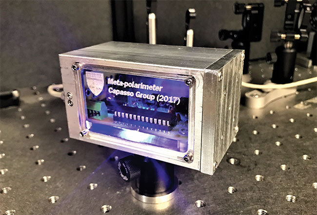
Figure 5. A plug-in prototype laboratory-grade polarimeter can read the polarization state of impinging laser light. Featuring a nanofabricated metasurface mounted in the faceplate on the right, the device has the potential to be manufactured at chip scale. Courtesy of N. Rubin/Harvard SEAS.
At the Harvard John A. Paulson School of Engineering and Applied Science (SEAS) in Cambridge, Mass., researchers applied another type of dielectric metamaterial to demonstrate a breakthrough polarimeter prototype6. Professor of applied physics Federico Capasso and colleagues used rectangular titanium dioxide (TiO2) pillar nanostructures to create a diffraction grating (λ = 532 nm) with polarization function built in (Figure 5).
Graduate researcher and first author on the published Optics Express paper, Noah Rubin, said the move toward dielectric materials such as dimorphic silicon reduces the losses that metal is known for. The performance of the prototype polarimeter is commensurate with commercial breadbox-sized versions based on wave plates, but the device is theoretically manufacturable by the millions at chip scale via cheap lithography. Challenges remain, however.
“The electron beam lithography used in this design becomes impractical for large areas,” said Rubin. “A lot of work remains, but the work is ongoing.” The field of polarization-resolved imaging could benefit from such a thin polarimeter material in applications such as medical diagnostics, machine vision, and resolving details through fog and water.
Said Brongersma, “Numerous industries are ripe for disruption. If we can finesse the mass production of these wafer-thin, lightweight optical metasurface solutions on large areas, they can be applied to surfaces of glass, semiconductors, and plastics to create new optical functions for these materials. I believe within the next year or two we will see several of these new materials become practical.”
According to Hu, more esoteric research and development efforts such as plasmon lensing will take years to come to commercial fruition, if they ever do. Adds DeGroote Nelson, the gap between hyped-up innovation and commercial reality can only be bridged by an enabling technology in another field such as optical and materials manufacturing. But the cycle is much shorter today with instant global information sharing.
“It took centuries for Leonardo da Vinci’s vision of the self-propelled cart to ultimately come to fruition at Ford Motor Company,” said DeGroote Nelson. “Nowadays, thanks to the fast exchange of information, the time it takes for the great ideas of visionaries to match up with innovative enabling technologies is much shorter. The materials we’re imagining today may rise to practical use in a matter of years.”
References
1. C. Soukoulis et al. (2008). The science of negative index materials. J Phys Condens Matter, Vol. 20, 304217, https://doi.org/10.1088/0953-8984/20/30/304217.
2. H-T. Chen et al. (2016). A review of metasurfaces: physics and applications. Rep Prog Phys, Vol. 79, 076401, https://doi.org/10.1088/0034-4885/79/7/076401.
3. Q-T Li et al. (2017). Free-space optical beam tapping with an all-silica metasurface. ACS Photonics, Vol. 4, p. 2544, https://doi.org/10.1021/acsphotonics.7b00812.
4. J. Hu et al. (2017). Evolutionary design and prototyping of single crystalline titanium-nitride lattice optics. ACS Photonics, Vol. 4, p. 606, https://doi.org/10.1021/acsphotonics.6b00955.
5. D. Wang et al. (2018). Stretchable nano-lasing from hybrid quadrupole plasmons. Nano Lett, Vol. 18, p. 4549, https://doi.org/10.1021/acs.nanolett.8b01774.
6. N. Rubin et al. (2018). Polarization state generation and measurement with a single metasurface. Opt Express, Vol. 26, Issue 17, p. 21455, https://doi.org/10.1364/OE.26.021455.