Sharone Zehavi, Scifiniti
Marrying the low cost of thin-film and the efficiency of crystalline silicon helps to improve solar cells.
The solar industry is at another inflection point in its development. Costs have come down as a result of a significant increase in capacity, and those reduced costs have caused demand to grow. The photovoltaics (PV) industry continues to work on improving the economics by developing new solar cells that maximize efficiency but are not too costly to produce, with the goal of reducing the levelized cost of electricity.
Crystalline silicon (c-Si) is the dominant technology and delivers the best efficiency, but the silicon wafer is the most expensive component in solar cell production. Thin-film technology has shown promise primarily because of its projected low cost, despite its lower efficiency. However, the rapid decline in price of c-Si cells, combined with rapid improvement in efficiency, has pushed thin film to the sidelines.
What if there were a third option – a process that would enable the development of solar cells that combine the low cost of thin film with the efficiency levels attained by c-Si? This third option does exist, in the form of new solar wafer technology that takes a different approach to development: depositing and crystallizing a layer of silicon on a low-cost conductive substrate. This process will cut manufacturing costs in half compared with current multicrystalline wafer costs, while delivering comparable efficiency.
Crystalline silicon dominates
Today, c-Si is the predominant material for developing solar cells, accounting for an estimated market share percent of 80 to 90. There are several reasons why c-Si is in such widespread use. Manufacturers developed a significant amount of practical experience and a lot of process technology through the use of c-Si in the microelectronics industry, and the entrenched, high-capacity infrastructure enables cost-effective production. Crystalline silicon yields solar cells with efficiencies ranging from 17 percent to as high as 24 percent. Multiple improvements have been made to reduce the cost and improve the efficiency of the solar cell, as well as the overall supply chain.
There are two types of c-Si used in the industry today: monocrystalline and multicrystalline. Monocrystalline is made by slicing wafers, up to 150 mm in diameter and 200 µm thick, from a single high-purity boule. Multicrystalline silicon, which is the bulk of the industry, is made by sawing a cast block of silicon first into bricks, and then into appropriately sized wafers.
The elusive promise of thin film
Another type of solar technology – thin-film PV – initially held a lot of promise in the industry. Many expected that, in the long term, thin film would surpass the dominant, conventional c-Si technology and, with lower end costs, achieve the clean-energy production objective of grid parity.
Thin-film solar cells are made by depositing one or more thin layers of a photovoltaic material on a substrate, with thicknesses ranging from a few nanometers to tens of microns. The cells can be made with a range of PV materials using various deposition methods on many different substrates. Commonly used materials include amorphous silicon (a-Si) and other thin-film silicon (TF-Si), cadmium telluride (CdTe), copper indium gallium selenide (CIS or CIGS), dye-sensitized solar cells (DSCs) and other organic solar cells.
However, the cost and complex processes required to make thin-film cells – and their comparatively lower cell efficiency – have impacted the widespread use of this technology. There is no established supply chain for producing thin-film cells, and each company is trying to develop its own processes and equipment, which adds cost and time-to-market disadvantages.
“Judging from recent price quotes, silicon thin-film price quotes [are] at US$0.58/watt, while silicon module is at US$0.60/watt. [The] price difference has decreased from the original US$0.10/watt to US$0.02/watt. Therefore, silicon thin-film product no longer holds price competitiveness,” wrote Arthur Hsu, research manager at EnergyTrend, a research division of TrendForce, in a May 2014 report. “Meanwhile, silicon module conversion efficiency is around 17.2 percent, while silicon thin film remains at 8 percent to 10 percent. [The] efficiency gap between the two will continue to increase as silicon module efficiency goes up.”
EnergyTrend has long been pessimistic about the future of thin-film products, mainly because the overcapacity of c-Si modules has put downward pressure on prices and left thin-film manufacturers little room for price negotiations. In fact, this pessimism appears to be warranted, as many thin-film manufacturers – such as DuPont, Honda Soltec and Oerlikon – have ceased operations.
Combining the best of both worlds
While c-Si maintains its dominance and thin-film technologies wane, a new generation of silicon wafers on the horizon shows promise in delivering silicon-level efficiencies at a lower cost, as thin film was expected to achieve. Designed using a different approach to manufacturing, the production technology for this new type of wafer can circumvent the major shortfalls of current wafering processes, driving the wafer cost down by 65 percent while delivering efficiencies that are comparable or better.

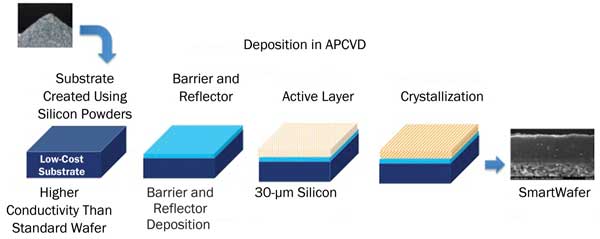
Figure 1. A continuous, atmospheric process deposits a 30-µm layer of crystalline silicon on a conductive substrate to reduce solar cell costs. APCVD = atmospheric pressure in chemical vapor deposition.
Developed from the ground up, this new approach takes into account the features needed to produce an efficient, cost-effective solar cell – such as a thickness that enables it to be strong enough to prevent breakage and to be processed through a high-volume manufacturing line – and also the amount of silicon required to deliver the photovoltaic effect. Also considered were the cost of capital, focusing on the need to avoid having to change manufacturing technology or purchase new equipment, and the operating expenses that are driven by consumables used during production.
The result is a low-cost, continuous, atmospheric process that deposits a 30-µm layer of industry-standard crystalline silicon on a conductive substrate (Figure 1). The ceramic-like substrate, which includes a barrier layer to prevent contamination between layers, is resistant to breakage, which improves yields in high-volume cell manufacturing using conventional equipment.
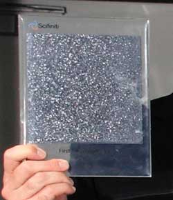
With this process, cell and module manufacturers will be able to utilize a wafer (Figure 2) that has significantly lower cost, offers the same or better efficiency over the long term, and works with back-contact cell, PERC (passivated emitter and rear contacts) and PERL (passivated emitter, rear locally diffused) designs. The design also provides for the capability to make n-type wafers and enables them to be used with heterojunction cells.

Figure 2. The resulting wafer has significantly lower cost than traditional wafers and offers the same or better efficiency over the long term.
Other cost savings result from reduced operating expenses, since no crucibles, wire saws or slurry are required. This new process will reduce capex to $14 million for 100 MW of production line, as compared with $60 million for standard c-Si wafers.
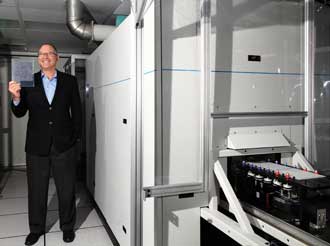
Looking ahead, this new wafer production method even shows promise for developing solar cells in larger form factors that can be applied in innovative designs (Figure 3).
Potential for the future
The market for photovoltaic power is becoming fiercely competitive in multiple countries, and in many cases, subsidies are no longer available to help encourage market growth and fuel greater deployments. With the success achieved to date, the market for solar modules is largely commoditized and consolidating, and only the most cost-efficient suppliers will survive.
Many attempts have been made to adjust or reinvent the supply chain and reduce material costs, but those have achieved only incremental improvements to date. To impact overall costs at all stages of the supply chain, the best opportunity lies in the fundamental innovations in the underlying wafer technology.

Figure 3. Sharone Zehavi of Scifiniti holds up an example of the company’s wafer.
With promises of lower price points, reduced capex and opex, and greater efficiency, these next-generation silicon wafers have a significant opportunity to fuel greater momentum in solar adoption. Not only will the technology speed time to market for the new wafer production capacity, it also will provide better margins for solar companies, enabling them to have a stronger business case and grow their companies.
Meet the author
Sharone Zehavi is chairman, president and CEO of Scifiniti in San Jose, Calif.; email: [email protected].