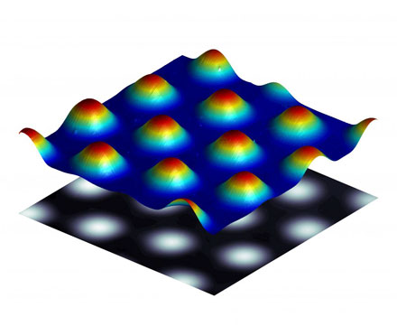
A method for patterning large areas with highly irregular structures in a single process aims to simplify the production of microlens arrays for photovoltaic systems and patterned films for other optical technologies.
To produce material arrays, the technique combines the highly regular convection pattern that forms in thicker material layers with strong interfacial deformations possible only in much thinner liquid films.
The resulting arrays locally enhance light intensity and could be used in integral imaging systems, unconventional photolithography and photovoltaic systems. For photovoltaics, an array of lenses placed atop a solar cell could serve as a light collector to enhance the efficiency of the photovoltaic system by making it less sensitive to the inclination angle of the solar light with respect to the cell surface. The method could easily be integrated into manufacturing lines, said researchers from the Technical University of Darmstadt who developed the process.

Illustration of the exploitation of cellular convection in a thick liquid layer to pattern a polymer film. Courtesy of Iman Nejati/TU Darmstadt.
"Unlike previous work addressing systems with several interfaces, in our approach each layer has a vastly different initial thickness than the other," said doctoral candidate Iman Nejati.
The approach involved sandwiching a thin film of oil that's sensitive to irradiation with UV light between a solid planar substrate and a much thicker layer of another immiscible liquid. The system therefore contained not only a liquid-gas interface but also a liquid-liquid interface.
"Exposing this multilayer system to a surprisingly small temperature difference in the direction of the layering causes stresses at the liquid-gas interface because of a temperature-dependent surface tension," said Nejati. "These stresses drive rotating cellular flow patterns in the thicker layer, which are highly periodic in the spread direction of that layer."

Rather than using the stresses caused by the temperature-dependent surface tension directly to pattern the film, the group's approach relied on the flow pattern in the thicker layer to deform the thinner film beneath.
The strategy enabled patterning of large areas with highly regular structures in a parallel — meaning all structures were fabricated at the same time — in a single process step, which saves time and reduces costs. Since the structures were generated from a liquid, without tools making mechanical contact with the working material, the resulting surface was very smooth and didn’t require additional processing.
By engineering the temperature distribution along the liquid-gas interface of the thicker layer, the convection cells and deformation of the thin film can be adapted to meet the specifications of a desired structure of interest, the researchers said. Once the desired deformation is achieved, it's "frozen" in place by irradiation with UV light.
The combination of advantageous features of the technique could make it a superior film fabrication method to current methods, such as photolithography, printing and embossing.
"Given the relative simplicity of the equipment needed for our method, and how easily it adapts to specific situations, it can be used for manufacturing low-quantity products as well," Nejati said.
The researchers also said that in the future, there would be no need to solidify the structures by UV light; instead the array of lenses could remain in the liquid state, which would allow modification of the periodicity of the liquid lenses if, for example, the temperature difference driving the convection cells is varied, enabling tunable lens arrays.
The research was published in Applied Physics Letters (doi: 10.1063/1.4940366).