Simulation tools bring the complex physics of two-dimensional materials and plasmonics together in a way that could change the face of optoelectronic devices.
VALERIO MARRA, COMSOL INC.
Ever since a single-atom-thick film of graphite was first successfully synthesized back in 2004, graphene has been on a decade-long ride through applications ranging from photovoltaics and next-generation batteries to electronics.
While its electrical and thermal conductivity made it attractive for electronics, its equally interesting optoelectronic capabilities were initially overlooked. But it soon became clear that graphene has incredible potential as a transparent conducting electrode and could be an alternative to the commonly used indium tin oxide (ITO). Graphene offers comparable or better optoelectronic performance in addition to its mechanical strength and flexibility. Other potential uses are diverse, and include applications such as transparent conductors used in touchscreens and photovoltaics (Figure 1), lab-on-a-chip devices for the sensing of viruses or proteins, improved night vision, mid-IR imaging applications and solar cells.

Figure 1. Bendable and lighter smartphone and laptop screens are just one of the many applications of graphene. Others include energy, computing, engineering, and health technologies and devices. Courtesy of Purdue University.
In addition to optoelectronics, graphene’s star has shone particularly bright in photonics when it is used in combination with the field of plasmonics, the exploration of light on ever-smaller scales. Squeezing light into smaller dimensions is fundamentally challenging due to the diffraction limit. The use of plasmonics helps address this challenge and enables light confinement even at the nanoscale. This is achieved by coupling incident light into oscillations of electrons known as plasmons — hence the name plasmonics. Today, plasmonics is an active branch of photonics that deals with the efficient excitation, control and use of plasmons.
Graphene-enabled plasmonics
Computational nanophotonics efforts at Birck Nanotechnology Center, Purdue University, led by Alexander V. Kildishev, associate professor of electrical and computer engineering, have been leading the way in combining graphene with plasmonics to bring it closer to practical optoelectronic applications.

Alexander V. Kildishev, associate professor of electrical and computer engineering, Birck Nanotechnology Center, Purdue University. Courtesy of Purdue University.
The work of Kildishev and his colleagues deals with a fundamental problem in graphene research: the difficulty of fabricating high-quality, large-area graphene films. Until graphene production improves, Kildishev and his team are leveraging simulation tools to perform design and optimization of devices made from graphene.
Through both simulation and experimental testing, Kildishev and his colleagues have been able to demonstrate tunable graphene-assisted damping of plasmon resonances in nanoantenna arrays, which is important for designing tunable photonic devices in the mid-infrared range1. Since the mid-infrared is where fundamental vibrational resonances reside for a wide range of molecules, it is critical to have tunable plasmonic devices that work in that range for applications in sensing and imaging.
On the other hand, moving closer to even shorter infrared (IR) waves — the telecom range — is also of ultimate importance for telecommunications and optical processing. The group at Purdue has shown efficient dynamic control of Fano resonances in hybrid graphene-metal plasmonic structures at near-infrared wavelengths. Fano resonances are seen in the transmission of specifically coupled resonant optical systems. Researchers are currently leveraging the properties of Fano resonances for use in optical filtering, sensing and modulators (Figure 2).

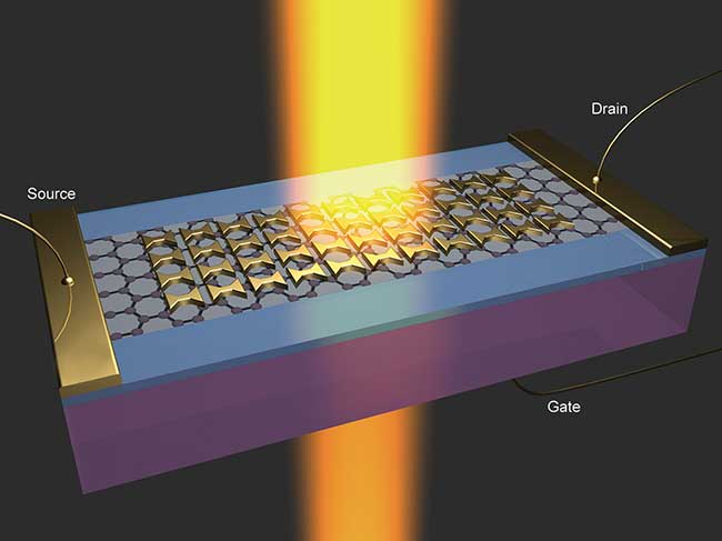
Figure 2. Design of Fano resonant plasmonic antennas on top of a single-layer graphene sheet optimized with modeling to achieve resonance at a 2-μm wavelength. The design tunability has been successfully validated in experiments using ion-gel top electrolyte gating2. Courtesy of Purdue University.
Leveraging the predictive power of Comsol Multiphysics software models is part of the team’s process for designing tunable elements for the next generation of plasmonic and hybrid nanophotonic on-chip devices, such as sensors and photodetectors. The photodetectors could ultimately find use in the sensing of infrared electromagnetic radiation for multicolor night vision and thermal imaging. Another application may be in biosensing, where the resonant lines of plasmonic elements are tuned to match the resonances of the spectral optical responses of viruses or proteins.
In their work, the Purdue researchers combined the unique properties of graphene with plasmonic nanoantennas to modulate the antenna’s optical properties. Having a tunable resonant element along an optical path is as critical to optoelectronics as having a transistor in an electric circuit.
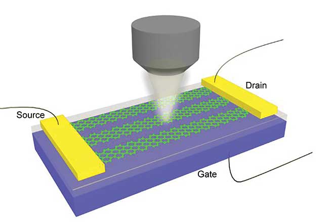
“By using the nanopatterned graphene with an electrical gating (Figure 3), it’s possible to modulate light flow in space with unparalleled spatial resolution,” said Naresh Emani, a former Ph.D. student advised by Kildishev, now with DSI, Singapore. “The reduced dimensionality and semi-metallic behavior of graphene plasmonic elements gives us, along with its other properties, a very vital feature — electrical tunability. This critical functionality is not attainable with conventional metal plasmonics.”

Figure 3. 3D artist’s sketch of the experimental setup used for studying plasmon resonance in graphene nanoribbons (GNRs), simulated with Comsol Multiphysics software using the surface current approach. The lattice orientation of GNRs is for illustration only and dimensions are not to scale.
Plasmonic devices based on noble metals lack this level of control over electrical tunability. Noble metals possess a large number of electrons in the conduction band, and consequently the electrical conductivity of metals cannot be easily modulated. But since graphene is a tunable semimetal, it does not contain any electrons in the conduction band in its pristine state. Therefore, its electron concentration — and hence its electrical conductivity — can be tuned chemically, modulated electrically, or even modulated optically.
The role of simulation and modeling
Numerical modeling has allowed researchers to optimize their designs without complications and the significant cost of nanofabrication processes.
“Compared to experimental work, mathematical modeling is low-cost, has the opportunity to validate its output through a reduced number of prototypes, has predictive power, and, finally, allows you to optimize for a desired functionality,” stated Kildishev.
In a field where the quality of the graphene material can vary, it is critical that there always be a tight connection between numerical results and experiments in order to better understand the impact of all variables involved.
In most cases, by fitting model parameters to experiments, Kildishev’s team can retrieve the actual physics of a given process. Having a validated mathematical model in hand always provides better understanding and interpretation. Once they understand the phenomena in terms of a mathematical model, the comprehensive knowledge of the whole mechanism can be applied to other new ideas.
Of course, mathematical modeling has its own barriers. Many problems do not have analytical solutions and Kildishev’s team must revert to alternative options.
This is where numerical techniques come in as tools for circumnavigating these hurdles, according to Ludmila Prokopeva, a high-performance computing specialist on Kildishev’s team. Properly designed simulation tools provide stability, accuracy and speed. There is often a need for substantial high-performance computational machinery, especially for nanostructured devices that require full 3D simulations.
The multiphysical and multiscale essence of computational nanophotonics necessitates the use of powerful simulation tools. It is never one simulation tool that works in all situations.
Kildishev’s team has a wide range of custom and commercial software, and they are always looking for ways to incorporate new and interesting physics. With Comsol software, the researchers can couple several physics interfaces sharing the same mesh or even having separate meshes. They also link the solvers to complex material functions, for example, implementing several complex dielectric models for graphene — written in MATLAB software. Some of these dielectric functions are impossible to handle for a straightforward explicit input in terms of plain arithmetic or look-up tables. They are also able to introduce nonlinear effects, couple these to a heat transfer analysis, and add quantum emitters.
Because of its atomic thickness, graphene behaves like a 2D material, but many researchers use a thin artificial thickness and have to resort to a 3D model in their simulations just because of the inability to treat 2D materials naturally in their software. The 3D approach brings unphysical shifts, uncertainty in optimization procedures and significant complications to the numerical calculations. The Purdue team was able to model 2D materials natively in terms of surface conductivity, such as surface current.
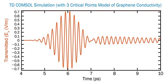
While waiting for manufacturing techniques to mature, the Purdue team used a theoretical model for graphene’s optical conductivity and simulated the device response to numerically investigate the system properties (Figures 2 and 4).

Figure 4. The time-dependent electric field of a Gaussian pulse transmitted through an array of graphene nanoribbons. Courtesy of Purdue University.
The experimental studies focused on very diverse facets of novel graphene applications, including IR sensors, hybrid photovoltaic electrodes and other 2D materials. So Kildishev’s team collaborated with their “next-door” experiment-oriented teams of professors Yong Chen, Alexandra Boltasseva, Vlad Shalaev, Ashraf Alam, David Janes and Gary Cheng at the Birck Nanotechnology Center at Purdue, and with the Ted Norris and Vinod Menon groups within the Materials Research Science and Engineering Center (MRSEC) at Purdue. The collaborations provided a base for validating new modeling approaches and feedback on the fabrication and optical characterization of real-life graphene-based nanostructures.
Looking ahead to quantum optics and flexible touchscreens
The Purdue team is continuing its simulation work to understand and predict the behavior of graphene so that it may be put to use in devices such as photovoltaics, optical modulators and — one day — flexible touchscreens. They are looking to make graphene nanoribbons so that they can begin fabricating a preliminary light modulation device3,4.
“Generation and modification of short optical pulses is an important aspect of imaging and sensing,” explained Kildishev. “Currently, the devices capable of achieving this functionality at mid-IR wavelengths are rather bulky and are not tunable. We envision a prototype device that can dynamically change the frequency content of an incoming optical pulse or light beam. This will enable higher sensitivity detection for night vision and mid-IR imaging applications.”
They also have longer-range aspirations to explore the plasmonic properties of graphene in the quantum optics regime. Kildishev and his colleagues believe the quantum optics regime will be the next frontier for the science of light and has been relatively unexplored in the mid-IR wavelengths.
“Semiconductor quantum wells show some interesting quantum properties but are restricted to low temperatures so far,” said Kildishev. “If we successfully address some of the challenges in graphene research, it might end up outperforming semiconductor quantum wells. If we are able to do this, we could significantly reduce the size of many devices.”
References
1. N.K. Emani et al. (2012). Electrically tunable damping of plasmonic resonances with graphene. Nano Lett, Vol. 12, pp. 5202–5206.
2. N.K. Emani et al. (2014). Electrical modulation of Fano resonance in plasmonic nanostructures using graphene. Nano Lett, Vol. 14, pp. 78-82.
3. D. Wang et al. (2015). Plasmon Resonance in Single- and Double-layer CVD Graphene Nanoribbons, in CLEO, p. FTu1E.3.
4. L. Prokopeva and A.V. Kildishev (2014). Time Domain Modeling of Tunable Graphene-Based Pulse-Shaping Device (invited), in ACES.
Meet the author
Valerio Marra is the marketing director at Comsol, where he leads the technical marketing group. His work combines technology, business and creative strategy to provide the Comsol community with the best technical content. Marra received a Ph.D. in fluid machines and energy systems engineering; email: [email protected].