Silicon may be mighty in electronics, but it’s puny in photonics – so far. Researchers have resorted to such tricks as combining silicon with other semiconductors or exploiting the Raman effect to coax out coherent light.
Silicon-based lasers could someday illuminate optics, link computer chips and power chemical sensors. Years of effort have led to recent advances – especially in hybrid lasers that marry silicon to other materials – that promise commercially viable silicon lasers sometime soon. Questions remain about the yield and reliability of such lasers, but testing and continued development now under way could address those concerns.
In hybrid lasers, the silicon is patterned to form a waveguide and, perhaps, part of the device cavity. The nonsilicon material forms the gain medium that amplifies the light, resulting in a laser.

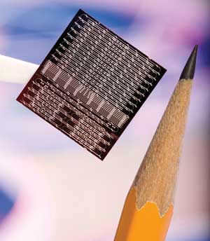
A transmitter chip uses hybrid silicon lasers and other photonic devices to send data at a rate of up to 50 Gb/s. Courtesy of Intel.
“The whole rationale for hybrid silicon lasers, meaning, in practice, a III-V semiconductor indium-phosphide-on-silicon laser, is to really use the best of two worlds,” said Roel Baets, a professor of photonics at Ghent University in Belgium. He also works at IMEC (International Medical Equipment Collaborative), a nanoelectronics research company based in Louvain, Belgium.
It is possible to produce a nonhybrid silicon laser, he added. This can be done using Raman lasers, as demonstrated by the Santa Clara, Calif.-based chip maker Intel Corp. some years ago. These lasers could form the basis for novel chemical sensors (see sidebar). Silicon-only lasers also can be built by four-wave mixing, a nonlinear phenomenon. However, both the mixing and the Raman approach require optical pumping, which makes such lasers a less than ideal fit for many applications.
Attention has therefore turned to the use of materials more suitable for electrically pumped lasers, such as indium phosphide (InP). In July 2010, Intel announced a 50-Gb/s optical link, with hybrid silicon lasers providing the light source for the connection. The device had four integrated hybrid lasers and four modulators, each running at 12.5 Gb/s. These multiplexed on the silicon chip and beamed out on a single optical fiber, producing 50 Gb/s in total.

Sticking the right stuff – such as lasing-friendly InP – to silicon creates a hybrid silicon laser.
One breakthrough that allowed the chip to be built was the development of a process that fuses InP to silicon. The technique also is vital to the commercial prospects of this approach.
“With one bond, I can create ‘n’ number of lasers. It’s a very highly manufacturable process, which means I can create lots of lasers per chip,” said Mario Paniccia, director of Intel’s Photonics Technology Laboratory.

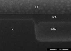
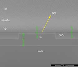
This cross section of bonding is done by means of a BCB
(benzocyclobutene) bonding layer. Courtesy of Roel Baets, Ghent
University.
At the InP emission wavelength of around 1.3 to 1.5 µm, silicon is a very low loss material, he said. Thus, when a thin layer of InP is bracketed by reflective Bragg gratings etched into silicon waveguides, light of a particular wavelength bounces back and forth, undergoing amplification on each trip through the InP. Lasing results when the gain exceeds the loss, at a wavelength determined by the resonant cavity’s construction.
This enables wavelength multiplexing, providing a path to boost data rates. For instance, moving from four to 16 channels would push the bandwidth to 200 Gb/s. The data rate per channel also can be increased through the use of faster modulators, such as 50-Gb/s devices; thus, links of 800 Gb/s – nearly a terabit – are on the horizon.
The hybrid laser platform can be used on everything from consumer products to high-performance computing, Paniccia said. In practice, it is likely to first appear in higher-end products because such applications will pay a premium for performance.
With a prototype device demonstrated, testing at elevated temperatures and voltages is under way, with the goal of determining the reliability and manufacturing yield of the lasers. This feedback will be used to tweak the process and correct problems. Although not releasing any specific data, Paniccia did say that the results so far look good.
In pursuing this hybrid silicon laser technology, Intel is working with companies such as Aurrion LLC, a privately held company in Santa Barbara, Calif., that makes hybrid silicon lasers and photonic integrated circuits. Fabrication is done in a standard CMOS (complementary metal oxide semiconductor) manufacturing facility, except for the application of the InP itself.
The company is commercializing the research of John E. Bowers, a professor of electrical and computer engineering at the University of California, Santa Barbara. Besides lasers, Bowers reported making resonators with quality factors upward of 28 million. This high quality factor means that these structures have an extremely narrow bandwidth compared with their center frequency, a useful attribute in various settings.
“Our goal is to take these really high-Q resonators and integrate them with lasers and detectors,” Bowers said.
Active research aims to cut the lasing threshold, with values as low as 2 mA achieved in ring lasers. Some of this work is being done in conjunction with computer maker Hewlett-Packard Co. of Palo Alto, Calif.
As for photonic integrated circuits, Bowers predicts that chips with thousands or tens of thousands of devices will appear within a year or two. The number of hybrid lasers on these chips will total far fewer than that, but such devices will still contain as many as 1000 lasers in a thumbnail-size chip.
These efforts to produce hybrid silicon lasers have been aided, in a way, by the demands of the semiconductor industry. Once exotic materials such as indium and phosphide are being used for electrical performance reasons in advanced chips, it makes their handling in CMOS much less of an issue than it would have been in the past. It also makes it more likely that layers of optical-grade indium phosphide will someday be grown or deposited on silicon, making it possible to perform the entire fabrication inside a single facility.
At the same time, semiconductor advances and research could give rise to another type of hybrid silicon laser. Last year, a group at MIT in Cambridge, led by professor Lionel Kimerling and senior research scientist Jurgen Michel, successfully prodded germanium into emitting telecom-wavelength laser light at room temperature. They did so by doping it with phosphorus and placing it on silicon in such a way as to create a strain in it.

Germanium lases when doped with enough phosphorus and strained by being attached to a silicon substrate. That allowed these chips to use germanium lasers to transmit data. Courtesy of Dominick Reuter, MIT.
An advantage of this approach is that germanium is much more compatible with silicon than III-V semiconductors, Michel said. That makes adding lasers based on germanium into standard manufacturing relatively easy.
“It’s just one additional process step you have to add,” he said. “It’s an additional two or three mask steps.”
However, in the original incarnation, these germanium-on-silicon lasers required optical pumping. Since that first report, the researchers have been working to increase the phosphorus doping level because that makes electrical pumping and modulation possible. They are close to reaching their goal, and Kimerling predicts that it will be achieved before summer is out. He also reported considerable commercial interest in the technology.

The silicon Raman lasers on this chip could power sensors by providing a source in the 2- to 5-µm range, achieving this by cascading the output of one to pump the next multiple times. Courtesy of Intel.
All hybrid silicon lasers have to confront challenges beyond yield and reliability. They also have to beat the competition, which is typically copper.
Take, for instance, computer interconnects. A growing amount of increasingly short-haul traffic travels over optical fibers, a long-running historic trend. Still, copper often finds a way to hang on.
A case in point can be seen in Intel’s new 10-Gb/s interconnect technology, Thunderbolt. Copper-based, it appeared for the first time in Apple computers in 2011. Years ago it was known as Light Peak, a name derived from the proposed optical interconnect. This change shows that copper can reach speeds and performance originally not thought possible.
At some point, copper will fail to deliver, and even consumer-grade applications will have to transition from electrons to photons, which is why cost and other issues of silicon-based lasers and other components are being addressed now. Exactly when that switchover will become mandatory is unknown, but expectations are that it will be soon.
As Paniccia said about Thunderbolt, “The next generation, whether it’s 20, 25 or 50 Gb/s, will have to go optical.”
Stepping Up to New Sensors
Although electrically pumped lasers are nice, getting to the right wavelength is sometimes more important. Take the case of sensors, where Raman lasers could shine if the right steps are taken.
In such lasers, an optical pump leads to stimulated Raman scattering and a laser output at a wavelength that is longer than the pump by an amount that depends upon the material. In the case of silicon, a 1550-nm pump results in 1686-nm lasing. If that output is cascaded into another silicon Raman laser, the second laser emerges at 1848 nm. Repeating the process could lead to lasing in the mid-infrared between 2 and 5 µm, a region with many molecular spectral fingerprints.
There are problems with silicon Raman laser cascading, one being potentially substantial losses during the multiple steps. Optimization may make these losses and other problems manageable, allowing the development of compact, low-cost, high-performance mid-infrared sources. The advantages of this for sensing applications could be significant, said Mario Paniccia, director of Intel Corp.’s Photonics Technology Laboratory.