Examining three facets of the micro-optics value chain — metrology, manufacturing, and application — sheds light on a field that is pushing boundaries in multiple sectors.
MARIE FREEBODY, CONTRIBUTING EDITOR
The transition of micro-optics from an emerging field into a cornerstone of modern optical systems offers considerable evidence in support of the commercial potential of light manipulated at microscopic scales. And, as the micro-optics technology space burgeons, an evolution is underway in the protocols spanning metrology, manufacturing, and applications. Today, biomedical devices, lidar, augmented and virtual reality (AR/VR), and telecommunications are among the sectors that are benefiting from breakthroughs in resolution, miniaturization, and functionality.
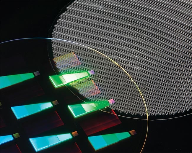
Courtesy of EV Group.
As it relates to broadening the commercial prospects for micro-optics, continued success depends heavily on sustaining the evolution of these protocols. Each of these areas — metrology, manufacturing, and application — presents distinct challenges and opportunities, ultimately shaping the future of optical technology from R&D all the way to the end user.
AR/VR, electronic devices, and imaging
Fundamentally, micro-optics surpass the performance capabilities of classical optics. For example, meta-elements and microlens arrays precisely manipulate the propagation of light at subwavelength scales. These optics can replace conventional bulky optics for compact, lightweight devices and enable new, and often novel, applications.
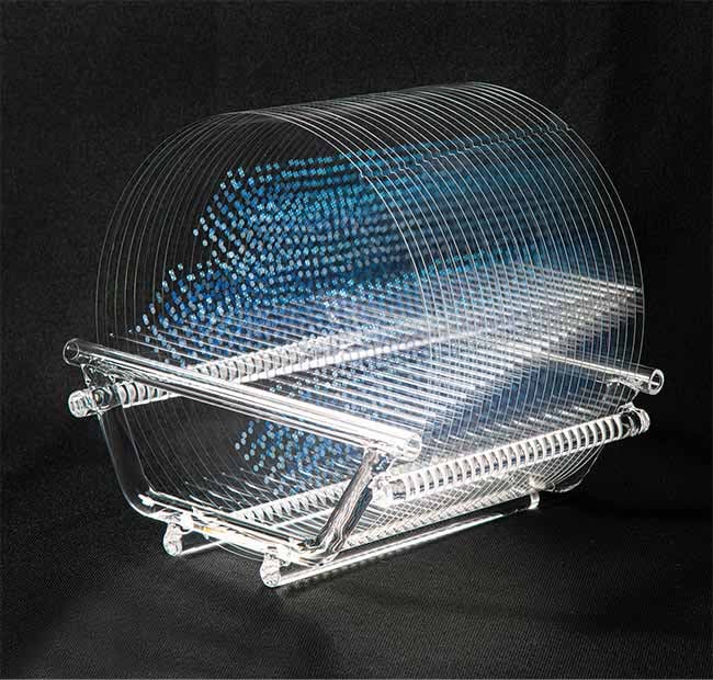
An increased demand for meta-optical
elements (MOEs) has brought manufacturing
methods, such as nanoimprint lithography (NIL),
as well as materials, into focus. Courtesy of EV Group.
These applications are flourishing in segments such as AR/VR and consumer devices. According to market research firm Yole Group, the progress of micro-optics can be tracked by investment amounts into emerging segments, including AR. One recent report revealed that micro-optics-focused startups that are expected to be part of the AR supply chain have received more than $300 million in investment since 2017.
Other consumer devices tell a similar story, though on a commercially accelerated scale.
“In smartphones and tablets, silicon-based metasurfaces will start to be integrated into 3D sensing modules for performance improvement or cost optimization,” said Yole Group technology and market analyst Raphaël Mermet-Lyaudoz. “With Apple making this choice recently, we can expect the company to integrate them into its entire product line, resulting in more than 100 million units per year,” said Axel Clouet, also a technology and market analyst with the firm.
AR/VR systems depend on micro-optics for immersive visuals. Microlens arrays and diffractive waveguides direct light from displays to the user’s eyes, minimizing distortion and maximizing field of view. Waveguides, in particular, project images onto transparent surfaces, blending digital content with reality. As AR/VR devices become increasingly sophisticated and user-friendly, the need for more advanced micro-optics is driving progress in design and manufacturing.
Still, there are obstacles to manufacturing at scale. Today’s metasurfaces for certain imaging applications can be produced using standard semiconductor processes, with few bottlenecks in place to prevent demand from being met. However, producers of nano-imprinted AR components have yet to standardize a manufacturing process that balances optical quality, throughput, and cost. But for now, the pace of market growth is allowing the current capabilities to meet demand.
Beyond imaging, metasurfaces find use for advanced marking solutions, such as for authentication. Switzerland-based Morphotonix, for example, uses precise photonic crystal manufacturing to limit counterfeiting on metal surfaces. The company’s solution is based on nano-engraving metallic articles with a precision of 130,000 dpi. Morphotonix also molds chocolate surfaces with microstructures to generate eye-catching rainbow-colored holograms.
Diverse application potential
In the field of biomedical imaging, diagnostic devices including endoscopes incorporate microlenses and fiber optic components. These optics enable high-resolution imaging with minimal invasiveness, helping physicians diagnose conditions more accurately and with less risk to the patient. Further, the use of gradient-index lenses, which vary in refractive index across the optic, allows for focusing light in extremely tight spaces. This enhances the imaging capabilities of these tools.
In optical sensing, lidar systems, which feature in autonomous vehicles as well mapping systems, rely on micro-optics for necessary beam shaping, focusing, and directing. Micro-optics in lidars facilitate the function of the laser pulses to measure distance(s). By improving the precision and efficiency of these optical components, manufacturers enhance the resolution and range of lidar systems to make them more effective for real-time object detection and 3D mapping.
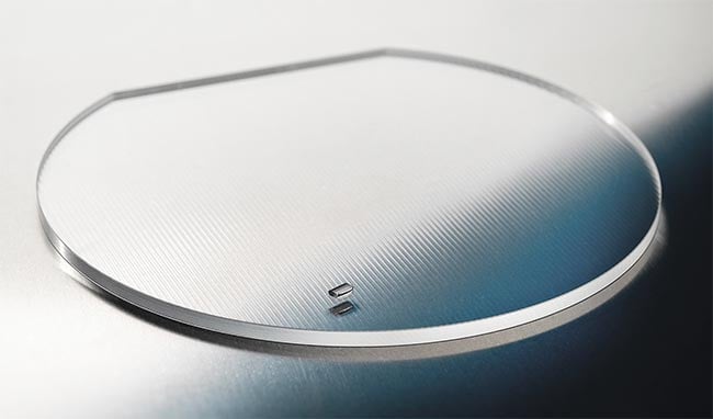
A fiber coupler array (the final product)
compared to a wafer (top). Both are made from
a glass with a high refractive index.
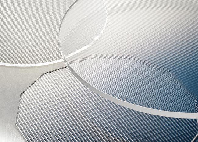
Offering a wide range of element sizes is crucial
to meeting the needs of various micro-optics
applications (bottom). Courtesy of Focuslight Technologies.
Micro-optics are also integral to advancements in telecommunications and photonics, particularly in fiber optics and PICs. Microlenses and beam-shaping optics are used to couple light efficiently between fibers and photonic chips, minimizing losses and improving signal quality. And in data centers, where speed and efficiency are paramount, micro-optics help to optimize light transmission through densely packed optical networks to ensure a faster and more reliable transfer of data.
Metrology tools and technologies
As micro-optics become more complex and their applications more demanding, the challenges in metrology will mount. The questions and objectives for experts will surpass those pertaining to measuring form or surface roughness. Rather, they will focus on solving complex problems that arise from different material properties, surface geometries, and wavelength-specific performance criteria.
Specialized tools and techniques are needed to perform accurate characterizations for each of these considerations. White light interferometry is a preferred technique for noncontact measurement, whereas confocal microscopy systems are particularly useful to evaluate steep surface angles and intricate geometries.
“For classical optics, which typically range from 0.5 to 4 in. in diameter, conventional test procedures are sufficient,” said Dirk Hauschild, senior strategic marketing expert at Focuslight Technologies. “However, micro-optical elements, particularly when produced in large arrays, require specialized parallel testing not commonly used [for] classical optics.”
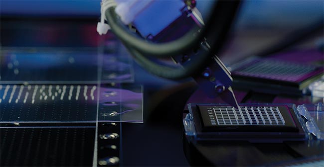
A fully automatic pick-and-place machine
can streamline crucial steps for high-volume
production. Courtesy of Focuslight Technologies.
Wavefront sensors are used to assess optical performance, measure light propagation, and reveal aberrations, focal quality, and diffraction effects. In this metrological setting, wavefront sensing ensures that the optics perform as designed, particularly for laser-based applications and optical communication systems in which wavefront integrity is critical. In partnership with a measurement tool provider, Focuslight Technologies enhanced its systems to measure the thickness of 300-mm wafers, enabling precise calculation of optical path differences in high-numerical aperture diffraction-limited microlenses. This allowed for the generation of simulations and performance maps, helping customers verify the repeatability and reproducibility of its components.
But in these cases, even the selection of surface file data formats can lead to errors in production, as well as in quality control — which is an element of manufacturing in which metrological considerations are highly prioritized. A challenge lies in minimizing systematic surface errors with the use of precise metrology. Injection molding, for example, is a common method for manufacturing micro-optics components that requires precision metrology at every stage of production. Equipment providers, such as New Hampshire-based Precitech Inc., use both in situ and post-fabrication metrology to ensure that lens molds meet the necessary tolerances for the target manufacturing steps.
Material-driven metrology challenges
Much like how the requirements of an optical element vary depending on application, different materials introduce unique metrology requirements. For example, the use of glass — widely favored for its optical clarity and broad wavelength transmission — requires metrology solutions to measure its surface roughness and form within nanometer tolerances. Yet since the transparency and high refractive index of glass makes surface measurement challenging with conventional profiling tools, interferometry with phase-shifting techniques is commonly used to measure surface form and wavefront error.
Polymers are popular in micro-optics fabrication for their cost-effectiveness and ease of manufacturing, especially for high-volume production. However, polymers pose challenges in terms of thermal stability and deformation. This means that metrology systems must assess initial quality and account for material creep or dimensional changes. Coherence scanning interferometry is often used in such cases to evaluate surface texture, step height, and material consistency across different batches.
Crystalline materials, such as silicon and gallium arsenide, are used in PICs, and their utility extends to infrared applications. These materials pose distinct challenges in birefringence and anisotropic etching behaviors. In one example, Sony Digital Audio Disc Corporation uses white light interferometry as well as atomic force microscopy to meet the required tolerance levels for light transmission and reflection.
AI in metrology
The integration of automated systems into production lines is underway throughout manufacturing. Real-time monitoring during fabrication enables quick adjustments, enhancing production efficiency and ensuring that each component meets the necessary and often rigorous specifications.
To maintain the quality and performance of micro-optical components, wafers, and stacks of thin substrates, solutions such as Äpre Instruments’ phase-shifting and spectrally controlled interferometers must provide real-time feedback to allow manufacturers to make immediate adjustments.
“Eliminating back surface reflections with [spectrally controlled interferometry] greatly shortens the feedback loop, as required in automated metrology,” said Robert Smythe, president of Äpre Instruments Corporation.
The incorporation of artificial intelligence (AI) also serves as a direct link between increasingly advanced metrology systems and practices, and sophisticated micro-optics.
“By integrating advanced automation and AI-driven metrology into the production line, manufacturers can ensure lenses meet quality standards while reducing costs and waste,” said Peter de Groot, scientist emeritus at Zygo Corporation. “Focusing on modular and adaptable systems allows companies to future-proof their investments and remain agile in the face of new challenges.”
Beyond standard wafer-level
Wafer-level fabrication techniques such as nanoimprint lithography (NIL) and photolithography, are well established in the manufacturing of micro-optics. However, innovations in the broader field of manufacturing technology are developing past standard processes, particularly as demand increases for more complex geometries, higher throughput, and multifunctional optical elements.
In response, new-to-develop approaches to manufacturing place a premium on increasing flexibility, improving scalability, and incorporating more materials into the fabrication process. Silicon-based metalenses, for example, are typically produced using traditional semiconductor processes such as ultraviolet (UV) lithography and etching. Diffractive optical elements use nanoimprint techniques, which enable high-volume manufacturing and are compatible with polymer-based resists.
In contrast, laser-based structuring, which uses ultrafast laser pulses to directly write optical structures onto materials, provides the flexibility to create custom patterns without the need for masks or molds. Laser-based structuring is especially suitable for prototyping or low-volume production of specialized optics as a result.
Other techniques support individual aspects, or process steps of the micro-optics manufacturing operation. The integration of multiple materials within a single optic, creating hybrid systems that combine the benefits of different substrates, is one trend that requires advanced bonding techniques and precision alignment processes. For example, glass microlenses can be combined with polymer-based diffractive elements to produce optics that can handle broadband light and offer superior diffractive properties. In this case, the bonding and alignment are vital to ensure that optical performance is maintained without introducing unwanted stresses or distortions. When fabricated to meet target specifications, such hybrid optics open possibilities for complex light manipulation in compact systems.
“There is a continuous push toward higher levels of integration,” said Thomas Achleitner, business development manager at EV Group (EVG). “At EVG, we are imprinting photonic structures on photonic integrated circuits, CMOS sensors, and next-generation displays. Accurate pattern fidelity and [having] full control of residual layers and the optical elements are prerequisites to address the demanding markets.”
Achleitner also emphasizes the importance of NIL for alignment accuracy, where sub-300-nm precision is often required for high-integration projects. In general, smaller elements are made using manufacturing technologies that have either been developed for, or are now found in, semiconductor manufacturing environments.
In current nanoimprinting tools, the alignment of multiple imprints, such as front-to-back surface(s), is typically within 1 µm. This alignment accuracy is determined by the aperture size, which is several microns or larger, rather than the smallest feature size, which can be as small as 50 nm.
According to Achleitner, another trend in recent years has been a significant push toward meta-optical elements. These elements feature a structured high refractive index surface, and the millions of meta-atoms that compose the surface of each have critical dimensions of only a few tens of nanometers with very high aspect ratios. Manufacturing such components, Achleitner said, requires sophisticated manufacturing technology that is typically only found in semiconductor manufacturing.
Ultimately, the intended application is the critical factor for determining key parameters. For imaging applications, the modulation transfer function is paramount. For meta-optical elements, lens efficiency takes precedence.
Up to scale
In terms of scalability, techniques such as glass reflow molding, as well as laser-based structuring, are helping to advance wafer-level optics manufacturing. Glass reflow involves heating glass to a specific temperature, at which it softens and conforms to a prefabricated mold. This enables the mass production of highly precise microlenses and optical components directly on a wafer.
Sony Digital Audio Disc uses high-volume injection molding and NIL to produce micro-optical components, such as diffractive optical elements, microlenses, and gratings with complex geometries that are fabricated on full polymer wafer substrates. Although the company is currently focused on development projects, it is aiming to become a provider of polymer micro-optic fabrication solutions, with mass production to follow.
“After 37 successful years in the entertainment industry, we are now establishing our partly unique production technologies and processes in the field of refractive and diffractive micro-optics and photonics,” said Rudolf Ablinger, manager of product and service development at Sony Digital Audio Disc. In addition to the manufacturing processes, Ablinger said the company is producing and using various coating processes for the planned undertaking.
Reducing barriers to entry
The success of micro-optics in core application areas such as biomedical, automotive (optical sensing), and AR/VR has increased the installed base for micro-optics production equipment. This in turn has allowed the ecosystem to develop predominantly with existing production capacity. Consequently, the entry barriers for production capabilities, such as NIL and UV molding, are decreasing.
As these barriers decrease, manufacturers are deploying high-precision robotic systems to align and assemble micro-optical systems with micron-level accuracy. These systems often incorporate real-time metrology feedback loops, enabling the manufacturers to adjust parameters such as pressure, temperature, and alignment based on immediate measurement data. This level of control minimizes human error and significantly improves yield, especially in high-complexity optics where even small deviations can lead to performance losses. Automation has also moved forward into post-fabrication processes, such as coating and packaging, where robotic systems ensure consistent quality across large production volumes. For micro-optics used in sensitive environments, such as medical devices or space applications, hermetic sealing and precision coating is critical.
“We are just at the beginning of how to make engineering of products and processes using the benefits of photons,” Focuslight Technologies’ Hauschild said.
“LED and laser in combination with micro-optics [have] already changed our lives and will be a solution for many challenges that we will face in the future. And it will be maybe one of the tools needed to bring and keep this planet in a good shape for coming generations.”