Dr. Dirk Mueller and Dr.-Ing. Oliver Haupt, Coherent, Inc.
In several industries, an increasing need exists to cut, drill and mark glass, sapphire and diamond – materials that are difficult to machine using traditional mechanical methods due to their brittleness and hardness. Their transparency at visible and near-infrared wavelengths has also made them a challenge to process using lasers. Now, industrial solid-state lasers with pulse widths in the subnanosecond domain can perform a variety of operations on these materials.
Short-pulse processing benefits
In laser micromachining of numerous different materials, shorter pulse widths have proved to deliver better results in terms of higher spatial resolution, better depth control, enhanced edge quality and minimized peripheral thermal damage. Several reasons account for this. The first relates to the fact that every material has an ablation threshold (the minimum peak intensity required to vaporize and remove material) related to pulse duration. Reducing the pulse duration generally reduces the ablation threshold. This means that the required pulse energy decreases as the pulse duration decreases. The advantage of this is that a lower pulse energy leads to less unwanted heating. A second benefit of shorter pulse widths is that more of the absorbed laser energy is carried away within the ejected, vaporized material before it can flow into the surrounding material.
For ultrafast pulse widths, namely those at the 15-ps range and below, the laser-material interaction operates on a mechanism that is fundamentally different from the mechanism that occurs with longer pulses. Specifically, longer pulses remove material through a photothermal interaction in which material is heated up until it vaporizes. In contrast, ultrafast pulses remove material by photoablation. In this process, the high peak fluences drive multiphoton absorption, stripping electrons from the material, which explodes away because of Coloumb repulsion. Because photoablation involves directly breaking the molecular or atomic bonds that hold the material together, rather than simply heating it, it is intrinsically not a hot process.
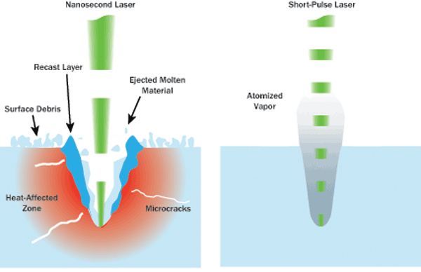
Figure 1. Ultrafast lasers remove material by photoablation, in which atomized material carries away most of the heat, resulting in essentially no heat-affected zone.
The primary limitation of short-pulse processing is that it typically provides lower material-removal rates, and ultrafast lasers have been more costly than long-pulse laser sources. As a result, ultrafast processing is typically reserved for applications demanding the greatest possible precision and quality, but the smallest heat-affected zone. Some of the most important of these are in the processing of glass, sapphire and diamond, which can be difficult to accomplish using other means.
Glass and sapphire cutting
The touch screen has become the dominant input method for a variety of consumer microelectronic devices, such as cellphones and tablet computers. The explosive market growth for these products has, in turn, fueled a tremendous demand for cutting thin glass sheets.
There are several important trends in touch-screen display glass cutting. One is a drive toward using thinner glass substrates to minimize the total weight of the display. Another is a need to cut curved shapes in the glass, rather than simply straight lines, to allow rounded edges on the display, as well as to accommodate more complex screen geometries.
As the display glass gets thinner, it is also critical that the finished product retain the ability to withstand being dropped, handled roughly and pressed upon (for touch screens). A typical LCD touch screen actually contains four stacked layers of glass. The topmost (outer) sheet is often a 700-µm-thick protective cover glass. To minimize the risk of scratching and breakage, this outer layer of the topmost glass is chemically treated to produce a very tough surface (Corning’s Gorilla Glass is an example of this). The thickness of this strengthened layer typically runs tens of microns deep.
Traditional mechanical glass cutting doesn’t work well with substrates under 1 mm thick. It produces microcracks, creates debris and leaves significant mechanical stress in the finished edge. All these problems necessitate further post-processing. This problem is further exacerbated with chemically strengthened glass, which is even more difficult to cut mechanically, especially at economically viable speeds.
Laser glass cutting has been in use for some time in the display industry. This is primarily accomplished with CO2 lasers; they rapidly heat the substrate, which is thermally shocked with a spray of air or water to create a crack that propagates through the thickness of the substrate. However, processing based on CO2 lasers does not work well for cutting curves.
More recently, a new laser-based micromachining method, referred to as filament cutting, has been demonstrated. Originally pioneered by Dr. Peter Herman and Dr. Abbas Hosseini of the University of Toronto, filament cutting has been commercialized by systems builders such as Innolas Systems using a 1064-nm laser with a pulse width of 15 ps.
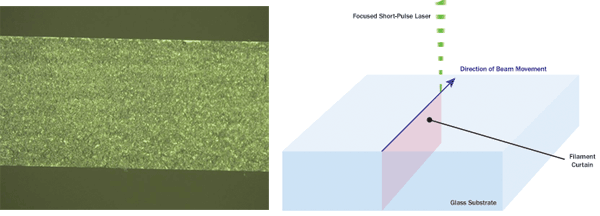
Figure 2. Filament cutting enables strengthened glass to be cut in a single pass, as shown here schematically. The photo at left shows magnified details of the high quality of the resulting cut edge.
With this technique, a tightly focused laser creates a “filament” within the material. Specifically, the high intensity of the ultrafast pulse induces the Kerr effect, resulting in a change in refractive index within the medium, which causes self-focusing of the beam. The filament can extend through the entire thickness of the glass and generate a plasma, which causes dissociation of the material, rather than removing it.
Filament cutting delivers the requisite speed and spatial accuracy, and yields superior edge quality that requires only minimal post-processing. Plus, the process speed is largely independent of the thickness of the chemically strengthened layer. For example, with a Coherent Hyper Rapid laser, 700-µm strengthened glass can be cut at up to 1000 mm/s, leaving edges with a groundlike surface roughness of less than 2 µm and excellent bend strength. Moreover, it can produce tight curves to enable simultaneous processing of holes and slots.
This novel technique can also be used to cut sapphire, which is often used for smartphone camera windows. Sapphire is even tougher than strengthened glass, and these windows must be cut with tight curves, as their typical diameter is around 5 mm.
Glass and sapphire marking
Lasers have been used for some time to mark glass. These marks can include text, logos, serial numbers and bar codes. The visibility of produced marks can be varied by adjusting laser parameters. This enables the production of clearly visible marks for aesthetic appeal or product personalization (e.g., putting an individual’s name on a product), as well as barely visible marks, such as might be used for anti-counterfeiting purposes (particularly important for medical products).
When laser marking glass, it is critical that the process not introduce any microcracks, as these can weaken the material and make it more subject to breakage. This is particularly problematic when processing strengthened glass products.
The newest technique in this area is so-called “color marking,” because the marks exhibit a rainbowlike color effect when viewed under the proper lighting. Color marking actually involves ablating just a few nanometers of material from the surface of a glass or sapphire substrate. Here, it is essential that the marking process produce a smooth variation in surface profile, without any cracks.
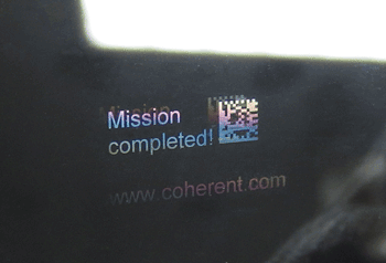
Figure 3. Color mark on glass, produced using a 700-ps laser (Coherent, Helios) operating at 532 nm.
A laser with a pulse width of 700 ps, operating at 532 nm, has proved effective for this process, whereas lasers with longer (nanosecond) pulse widths may cause types of damage that are not acceptable. In particular, this short-pulse width source enables a large process window for crack-free marking.
Lasers with pulse widths in the 700-ps range also are used to engrave and produce more traditional marks on glass and sapphire. In this case, marks are typically on the order of 10 µm deep to make them clearly visible. One particular application is in marking the sapphire wafers used as substrates in the production of high-brightness LEDs. The marks are typically lot numbers and other identifying information placed on the sapphire after LED structures have been created – i.e., after a significant amount of cost has been built into the substrate. The major challenge here is producing easily readable marks without having a negative impact on the surrounding circuit structures.
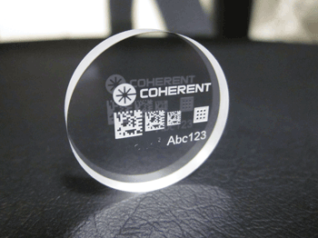
Figure 4. Picosecond lasers can mark sapphire, which is difficult to mark by other means due to its extreme hardness.
In the past, some sapphire marking has been performed with nanosecond lasers, but the quality is less than optimal, and these lasers can produce microcracks in the substrate. Marking with a 700-ps-pulse-width laser operating at 1064 nm solves both these problems and results in marks with excellent surface and edge quality, sharp detail and an absence of peripheral damage and recast material.
Diamond cutting
Diamond is the hardest known material, making it particularly difficult to machine using mechanical methods. Its high transparency from the ultraviolet through the far-infrared also makes it challenging to process using most lasers. However, diamond can be very successfully cut using lasers with pulse widths of 15 ps or less.
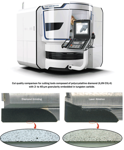
Figure 5. The EWAG Laser Line Ultra (above) is a system for fabricating diamond tools. The photos (below) compare a tool edge prepared using traditional diamond grinding with one produced using laser ablation. The laser-produced edge is smoother, with virtually no chips on the cutting edge.
One application for diamond cutting using ultrafast lasers is in the machine tool industry. Specifically, the laser can prepare the sharp edges of machine tool bits (e.g., drills and cutting bits for lathes and milling machines) consisting of a tungsten carbide substrate with embedded diamond granules. These diamond granules typically range from just a micron or two, up to tens of microns in size.
The noncontact cold processing achieved with the ultrafast laser removes material to produce a cutting edge that is high quality and free of chips. For substrates that contain relatively large diamond granules, the laser can even ablate a part of a diamond grain to maximize edge smoothness. This quality level is virtually impossible to achieve using traditional mechanical machining methods. Furthermore, laser processing enables the tool edge to be contoured with a precise shape; even concave forms can be achieved. The result is both enhanced tool functionality and extended lifetime, since it is well-established that slightly rounded cutting edges wear better over time than sharper ones, which have a tendency to chip.
Meet the authors
Dr. Dirk Müller is director of product line management for industrial ultrafast lasers at Coherent in Santa Clara, Calif.; email: [email protected]. Dr.-Ing. Oliver Haupt is senior product manager for industrial subnanosecond/pico-second lasers at Coherent in Germany; email: [email protected].