THOMAS ACHLEITNER AND ANDREA KNEIDINGER, EV GROUP (EVG), AND STEPHAN PRINZ, DELO INDUSTRIAL ADHESIVES
Polymer refractive microlenses are the core technology in many micro-optical modules, which themselves are critical enabling technologies for an expanse of optoelectronic systems, including those found in cars, smartphones, and wearables. Microlenses in ambient light sensors, diffractive optical elements for structured light generation, and high-precision surface relief gratings in diffractive waveguides — which enable emerging technologies such as 3D sensing and augmented reality glasses — are just some of the functionalities that these refractive optics enable. In the automotive sector specifically, this class of micro-optical modules is used in ultracompact microlens-enabled projector beam headlights and other lighting features, both functional and cosmetic, that can be found virtually anywhere in the car.
The current rise of polymer refractive microlenses points to a broader trend that is underway, with implications for fabrication technologies. Unquestionably, the increased adoption of micro-optical components and devices is necessitating robust and economic manufacturing. Today’s production requirements for hundreds of thousands or even millions of pieces each year command new and innovative solutions.
One such approach is UV lens molding. Unlike generic injection molding, used mainly for macroscopic elements, the UV lens molding process meets the stringent requirements of micro-optics manufacturing, specifically as it relates to alignment precision. Lens molding uses transparent working stamps to replicate defined lens shapes into UV-curable polymers — essentially, adhesive resins — directly deposited onto substrates, such as glass or silicone. To deposit the polymer, puddle or droplet dispensing is used. Subsequently, the working stamp, on a rigid backplane, is brought into contact with the substrate using a linear force. The rigidity of the backplane enables high alignment accuracies. The polymer is UV-cured to form a solid lens with glass-like properties.
Upon completion of this process, the working stamp is released and reused for the next batch of imprints. The imprinted wafer, which may contain up to thousands of optical elements, can now be further processed.
And, because the stamp structure is replicated in a single step directly into the material with UV-curing instead of heat, the lens molding and nanoimprint lithography (NIL) methods are significantly more sustainable than other lithography or replication technologies. Also, alternative lithography methods are limited in their ability to be used to manufacture complex optical structures at the wafer level. NIL and lens molding are insensitive to shape and complexity, rendering them suitable for high-volume production of almost any optical system.
The combination of NIL and lens molding not only enables miniaturization, but it also allows for monolithic integration and dense wafer-level packaging, which pushes this miniaturization toward new standards. NIL enables fabricators to create multifunctional optical systems, with the ability to combine polymers, each with different functionalities, in subsequent steps that must be completed during the imprinting stage.
Micro-optics application trends
UV lens molding is finding widespread application in direct imprint processes, replacing the traditional etching processes that previously dominated in these use cases. The UV approach is more efficient and sustainable in many instances and, in sectors including automotive (microlens arrays), UV lens molding comes with a higher reliability standard than legacy and/or alternative methods.
Additionally, as ongoing efforts in miniaturization often come with their own set(s) of strict criteria for any technical polymer that may be used in the assembly of ultrafine components, lens molding has become a mainstay in applications combining UV-curing and micro-optics fabrication. And with increasing market penetration now calling for higher production volumes, and an increasing degree of automation as a result, capacity is more efficiently upscaled with larger wafers with more units per hour rather than lengthening production lines and adding machinery.
In this context, a recent study led by DELO and partner EV Group (EVG) aimed to determine how UV-curable polymers can augment the manufacture of wafer-level micro-optics. As is well understood in the semiconductor industry, increasing wafer sizes can be challenging. This study demonstrated possibilities for settings beyond the controlled laboratory environment, in real-life production sites with state-of-the-art machinery and materials.
Study parameters
The collaborators used the EVG7300 multifunctional UV lithography system, which features an alignment accuracy of 300 nm and allows for easy production scaling with wafer sizes ranging from 150 to 300 mm. The machine enables nanoimprinting capabilities, including conformal printing, automated low-force stamp detachment, and fast curing times when paired with a high-performance curing lamp emitting at intensities >500 mW/cm2.
Through the course of the study, the collaborators achieved the simultaneous production of working stamps and imprints. This eliminated the need for multiple tools and allowed the study participants to bypass removal of the wafer from the system environment. The degree of automation at which stamps and substrates were handled could be customized per the user’s preferences with a selection of either manual, semiautomated, or fully automated modes.
The properties of the resin used for the study posed an additional consideration. Indeed, the properties of a resin used in a particular imprinting process can determine both the success of the imprinting process itself and the overall performance of the resulting optical element. The resin used in this case was a fast-curing epoxy-based polymer that can be universally used for lens molding in single lenses or microlens arrays as well as for the replication of nanostructured diffractive optical elements. When stamped, it showed minimal interaction with the stamp and low detachment force. These results indicate a long stamp service life and easily automated separation. A very low rate of volume shrinkage at 2.4% allowed for the exact reproduction of master geometries and smooth optical surfaces throughout the lens-molding process.
This resin additionally showed transmission values at ~100% over the entire visible spectral range with no scattering, indicating that it was optically clear. Optical stability was maintained, even after challenging reliability tests, which included a 3× reflow test, according to the JEDEC (Joint Electron Device Engineering Council) standard J-STD-020D.1, with a peak temperature of 260 °C, after 1000 h of storage at 85 °C and 85% humidity, and after 1000 h of storage at 125 °C under simulated sunlight (Figure 1).
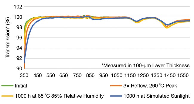
Figure 1. Transmission values at ~100% over the
entire visible spectral range with no scattering
were achieved, indicating that the resin was
optically clear. Optical stability was maintained,
even after challenging reliability tests, such as
reflow soldering or ‘85/85’ storage. Courtesy of DELO Industrial Adhesives.
Finally, the resin takes on compression shear values of >15 MPa on substrates, such as glass and polycarbonate, without any pretreatment or primer.
Study tests and results
A fully populated master with test lenses was used for replication tests. Standard glass with a thickness of 500 µm and an 8-in. diameter was used as the substrate; this glass is commonly used in wafer-level optics. After replicating the working stamp from the master, 10 wafers were imprinted with the material combination to undergo examination (Tables 1 and 2).
The first test examined optical quality. In this test, lenses were evaluated for cracks, bubbles, and shrinkage. No bubbles, cracks, or shrinkage were observed in/on the imprinted lens. The surface of the molded lenses did not change across all replication steps from master to final imprint. No uncured material or residue was observed on either lens, indicating completed curing. After undergoing measurement for volumetric shape fidelity, using a white light interferometer, results continued to show no cracks, bubbles, or shrinkage.
The measurement results indicate that the selected resin is suited for wafer-level optics applications, without creating any visible deformation, residue, or defects on the molded lens. Additionally, it can be fully cured without any further shrinkage.
A second test examined roughness. Ideally, the surface of a fully cured lens must demonstrate low surface roughness to achieve optimal performance across multiple end applications. How lens surface roughness changes over the course of wafer-level optics processes — from master to final imprint — is a crucial parameter.
Lens roughness in this study was measured using a white light interferometer. Five lenses from each step were measured: center, left, right, top, and bottom (Figure 2). The average roughness (RMSsurface) of the lens surfaces is <10 nm, representing a common requirement for optical active surfaces. The average surface roughness showed almost no change from master to imprints, and over multiple imprints. This indicator of process stability reflects how lenses molded with the resin showed constant surface roughness over the whole imprint series on a low absolute level. The material cured evenly, fully replicating the surface shape of the master, without adding additional defects or deformities. The curing and detachment of the material did not influence the surface quality of the wafer stamp mold, as seen in the stable roughness values of the imprint series.
Table 1.
Working Stamp Properties
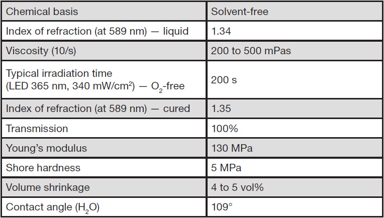
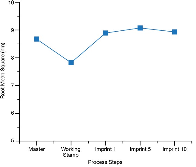
Figure 2. Obtained via white light interferometric measurement, the chart data shows lens roughness
values, from the surface of the master via the working stamp to final imprints. Five lenses from
each step were measured: center, left, right, top, and bottom. The chart shows the average values. Courtesy of DELO Industrial Adhesives.
A third test examined replicability by comparing the measured profile of the molded lens to the initial lens design equation. This comparison of the profile to the equation resulted in a residual error plot.
The principal parameters that derived from this residual error plot are peak-to-valley (PV) and root mean square (RMS). Here, PV is the difference in height between the highest and lowest points in the residual error plot, and it represents a worst-case scenario for the surface in this test. RMSresidual error is a method for describing the average deviation of the surface figure from the desired surface and describes the overall surface variation.
In testing the replicability of the lens profiles, the molded lenses were measured with an industry-standard tactile profilometer and analyzed for shape PV stability. Five lenses were measured from each step (master, working stamp, and imprint 3× (up to the 10th)): center, left, right, top, and bottom.
The measured profiles were overlaid and compared with the profiles from the metal master and wafer stamp. Each of the measured profiles showed a very uniform shape without any discrepancies. The lens profiles resulting from the imprint series with the adhesive used could be perfectly laid over each other. The study participants further observed no change in shape between the 1st and 10th imprint, which indicated a stable process and no deformations in the stamp mold.
In determining the residual error plots of the master, stamp, and imprint, each was calculated and compared by overlaying the plots. The resulting data shows that the plots are almost identical. This points to high fidelity in the replication throughout the entire process, resulting in favorable correlation to the above overlaid raw lens profiles.
Additionally, the residual error plots of the 1st, 5th, and 10th imprints were compared to see whether the imprint process itself was stable (Figure 3).
Table 2.
Lens Material Properties
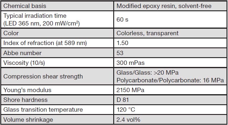
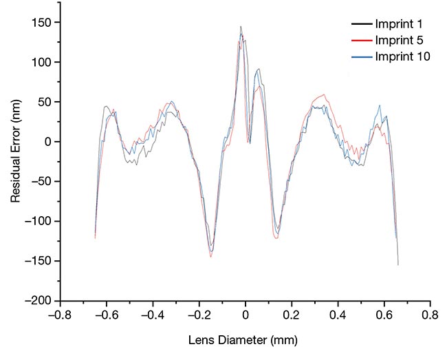
Figure 3. Residual error plots of 1st, 5th, and
10th imprints were compared, demonstrating
that the imprint process itself was stable. Courtesy of DELO Industrial Adhesives.
A comparison of the residual error plots from the 1st and 10th imprint showed almost no difference in the shape of the profile, indicating no significant change in the molded lenses between the start and the end of the automatic molding process, underlining their favorable reproducibility.
The increase and subsequent reduction of the PV and RMSresidual error value from the master over the working stamp to the imprint is due to the reversed polarity of the molded cavity and change in residual error. The precise PV and RMSresidual error values, calculated from the residual error plots, can be seen in Figure 4. Additionally, it is shown that the average absolute PV value of the imprint series with the resin used is as low as 330 nm with a stable RMSresidual error of ~55 nm, which is close to the value of the master. The minimal deviation observed is a result of material shrinkage. This offset can be easily considered in the master design and therefore compensated for.
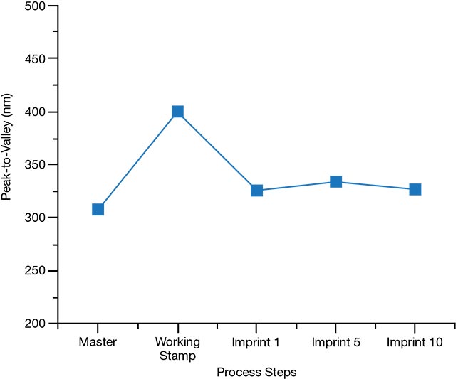
Figure 4. The charts show the precise peak-to-valley (PV) (a) and root mean square residual error
(RMSresidual error) (b) values calculated from the residual error plots. A comparison of the residual
error plots from the 1st and 10th imprint shows almost no difference in the shape of the profile
(Figure 3), indicating no significant change in the molded lenses between the start and the end
of the automatic molding process. Courtesy of DELO Industrial Adhesives.
Both the PV and the RMSresidual error values remain on a constant level over all imprints. The deviation range of the PV is well below 100 nm, and the RMSresidual error is <10 nm. Both minimum deviation ranges are an indicator for a stable and reproducible process.
A fourth test examined reliability, in which wafers were subjected to a reflow process three times, in accordance with JEDEC standard J-STD-020D.1, at a peak temperature of 260 °C. Visually and optically, the lenses showed no changes after the reflow process compared to the imprint series. No yellowing or cracking of the lenses was visible even after three administered rounds of reflow.
A profilometer was used again to measure the lens shapes after reflowing via the same procedure previously described. Figure 5 shows the overlaid error plots of the measured lenses after the reflow process, compared to the profiles after 10 imprints. The shape of the lenses is almost identical between the reflow steps and imprints. No deformation or deviation from the original shape is observed. Also, no significant change in height or diameter of the lenses is seen. Overall, the lenses showed high stability during the reflow process.
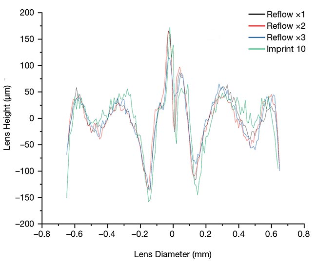
Figure 5. The chart shows residual error plots of the lenses following the reflow process,
indicating no significant change in the molded lenses. Courtesy of DELO Industrial Adhesives.
Consistent quality
The detailed analysis of the imprinted lenses molded with the chosen resin shows consistently high-quality lens shapes with consistently low surface roughness throughout the process chain. The lenses are not influenced in their shape by the reflow process in any significant manner. Additionally, the imprinted lenses show no measurable changes in transmission or mechanical behavior upon exposure to an additional reflow process. This demonstrates that the optics manufactured by lens molding are suitable for demanding packaging applications in optoelectronics, even satisfying typical automotive standards.