Scope Reveals New Physics of Graphene
GAITHERSBURG, Md., Sept. 8, 2010 — Using a one-of-a-kind scanning-probe microscope, an international team of researchers discovered that electrons in graphene, which comprise four quantum states, can split into different energies when exposed to extremely low temperatures and extremely high magnetic fields. The new research raises questions about the fundamental physics of graphene and reveals new effects that may make the material even more powerful than previously expected for practical applications.
While graphene is a simple material — a single-atom-thick sheet of carbon atoms arranged in a honeycomb-like lattice — its properties are surprisingly complex. Measuring and understanding how electrons carry current through the sheet is important to realizing its technological promise in wide-ranging applications, including high-speed electronics and sensors.

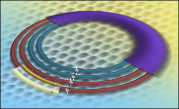
This artist's rendition illustrates the electron energy levels in graphene as revealed by a unique NIST instrument. Because of graphene’s properties, an electron in any given energy level (the wide, purple band) comprises four quantum states (the four rings), called a “quartet.” This quartet of levels split into different energies when immersed in a magnetic field. The two smaller bands on the outermost ring represent the further splitting of a graphene electronic state. (Image: Kelly Talbott/NIST)
For example, the electrons in graphene act as if they have no mass and are almost 100 times more mobile than in silicon. Also, the speed with which electrons move through graphene is not related to their energy, unlike materials such as silicon where more voltage must be applied to increase their speed, which creates heat that is detrimental to most applications.
To fully understand the behavior of graphene's electrons, scientists must study the material under an extreme environment of ultrahigh vacuum, ultralow temperatures and large magnetic fields. Under these conditions, the graphene sheet remains pristine for weeks, and the energy levels and interactions between the electrons can be observed with precision.
Scientists recently constructed the most powerful and stable scanning-probe microscope available at the National Institute of Standards and Technology (NIST), with an unprecedented combination of low temperature (as low as 10 mK, or 10 thousandths of a degree above absolute zero), ultrahigh vacuum and high magnetic field. In the first measurements made with this instrument, the team has used its power to resolve the finest differences in the electron energies in graphene, atom-by-atom.
"Going to this resolution allows you to see new physics," said Young Jae Song, a postdoctoral researcher who helped develop the instrument at NIST and make these first measurements.
And the new physics the team saw raises a few more questions about how the electrons behave in graphene than it answers.
Because of the geometry and electromagnetic properties of graphene's structure, an electron in any given energy level populates four possible sublevels, called a "quartet." Theorists have predicted that this quartet of levels would split into different energies when immersed in a magnetic field, but until recently there had not been an instrument sensitive enough to resolve these differences.
"When we increased the magnetic field at extreme low temperatures, we observed unexpectedly complex quantum behavior of the electrons," said NIST Fellow Joseph Stroscio.
What is happening, according to Stroscio, appears to be a many-body effect, in which electrons interact strongly with one another in ways that affect their energy levels.
One possible explanation for this behavior is that the electrons have formed a condensate — they cease moving independently of one another and act as a single coordinated unit.
"If our hypothesis proves to be correct, it could point the way to the creation of smaller, very-low-heat producing, highly energy efficient electronic devices based upon graphene," said Shaffique Adam, a postdoctoral researcher who assisted with theoretical analysis of the measurements.
The research team, led by Stroscio, includes collaborators from NIST, the University of Maryland, Seoul National University, the Georgia Institute of Technology, and the University of Texas at Austin.
The group described how the energy levels of graphene's electrons vary with position as they move along the material's crystal structure last month in Nature Physics. The way in which the energy varies suggests that interactions between electrons in neighboring layers may play a role.
The group's most recent work is published in the Sept. 9 issue of Nature.
For more information, visit: www.nist.gov
Published: September 2010