By: Brian Elias, director of engineering at Cal Sensors
The infrared region from 1 µm to 5 µ is an area of interest for both spectroscopic and thermographic applications. Lead sulphide (PbS) and lead selenide (PbSe) are intrinsically photoconductive materials that cover this important spectral region and have a long history of development and manufacturing. They have several advantages over competing materials, but because of their nature, they also have several challenges that need to be addressed. This article looks at the application of several established technologies that have been applied to make PbS and PbSe arrays compatible with modern infrared array applications. An implementation will be shown that takes advantage of these techniques to produce a second generation array.
A variety of detector materials can be considered for the small, low powered, low cost systems required today. Of these detectors, there are a number which typically operate at very cold temperatures to reduce thermally generated free carriers and achieve adequate performance. These include InSb, InAs and HgCdTe. These materials should not be considered unless the system performance requirements warrant the increased size, cost and complexity. Thermal detectors using pyroelectric or bolometric materials could be considered because of their broad wavelength response, however they have low sensitivity and slow response speed compared to photon detectors so they would be inappropriate for a general purpose spectroscopic or thermometric system.
The detector materials that remain for consideration are InGaAs photodiodes (both standard and extended) and lead salt photoconductors (PbS and PbSe). All of these have reasonable cooling requirements and good response times. Standard InGaAs photodiodes have excellent sensitivity and speed, but are limited in upper wavelength sensitivity to 1.7 µm and therefore can not be considered for a general purpose solution even in the near infrared. Extended InGaAs photodiodes have reasonable sensitivity, but still only extend to 2.6 µm. The remaining alternatives, PbS and PbSe photoconductors have characteristics that make them excellent candidates. PbS has detectivity values that are at least as good as Extended InGaAs with sensitivity to 3µm. PbSe is approximately an order of magnitude less sensitive than PbS, but has sensitivity to 5 µm.
History of Lead Salt Photoconductors
Lead salt photoconductors have a long history of development. The photoconductive properties of lead sulfide (PbS) were discovered in 1933 by Kutzscher at the University of Berlin, although his work was performed in great secrecy and not publicly known until after 19451. Lead sulfide was also produced by Cashman (Northwestern University) and Gudden (University of Prague) and implemented for various military applications at that time and indicated good sensitivity to 3 µm. Robert Cashman was also working with other lead salt compounds and showed that lead selenide (PbSe) also had promise as a photoconductor to 5µm, which was particularly important because of the 3 µm – 5 µm atmospheric transmission window. Commercial production of PbS began around 1943 in Germany, 1944 in the United States (Northwestern University) and 1945 in England (Admiralty Research Laboratory).
PbS and PbSe have a long history of development and have taken advantage of advances in manufacturing techniques to continue to be important detectors for infrared sensing. Advances in photolithography in the 1960s provided the methodology to create arrays of photoconductive materials, thereby advancing the number of applications available to these detectors particularly in the area of spectroscopy.
Principals of Photoconductivity
Photoconductors are essentially resistors whose conductivity changes with incident photons. A photon with energy greater than the material’s band-gap energy is absorbed in the photoconductive material to produce electron-hole pairs, which increases the conductivity of the material. To measure the incident radiation a simple voltage divider bias circuit is typically used. The current through the load resistor, and therfore the voltage across the load resistor varies with incident radiation. In practice the photoconductive change is small compared to the bulk resistance of the material, so differentiating the signal can be difficult. An AC coupled circuit is often used and the radiation source is modulated by mechanical (chopper) or electronic (pulsed source) means.
Besides providing the ability to easily distinguish the photocurrent, this method has the added advantage of minimizing the detector noise, including 1/f noise inherant in these detector materials, by use of a bandpass filter or lock-in amplifier centered at the modulation frequency. The disadvantage of the modulated source method is the size and complexity of modulating the source and the fact that slow or steady state radiation changes cannot be detected.
Because of the nature of photoconductive materials there are several issues that need to be addressed to insure a successful product. This is particularly important in applications that require high sensitivity such as reflective spectroscopy or precision thermography.
Thermal Coefficient of Resistance
Photoconductive detectors have a bulk resistance which is temperature dependent. For lead salt photoconductive films this temperature dependency is typically on the order of 3 %/°C. The problem is that if the bulk resistance is changing due to temperature variations it can be indistinguishable from the photoconductive signal. Modulation of the signal radiation can help address this issue, but this requires extra hardware and is not an option where modulation is not compatible or desired in the system solution.
Several schemes have been developed to attempt to compensate for the change in detector resistance and responsivity that occur as the temperature of the film changes. Some of these schemes include elements, such as per-detector thermal compensation elements, that are not compatible with large pixel count arrays. The most simplistic approach is to hold the detector temperature constant as the ambient temperature changes. Fortunately advances in Peltier cooling technology and cooler control design make it relatively easy to include a thermoelectric cooler, temperature sensing device, and control electronics2, 3 into any system solution. The solution chosen for this development was a thermoelectric cooler with a surface area large enough to encompass both the detector array and the interfacing electronics chip. Holding both the detectors and the electronics in an isothermal condition insures maximum stability in the device. Locating the sensing element as close to the center of the isothermal surface as possible improves the feedback to the control circuit.
'Dark' Current
As previously discussed, in the typical bias arrangement there is a bias or “dark” current generated by the bias voltage being applied across the bulk (dark) resistance of the photoconductor. Because the change in resistance due to photon generated carriers is small compared to the bulk resistance of the film, the signal current change is commensurately small. In order to detect the incident photons on the film, the bias current must be disposed of in some manner. This is often done, again, by modulating the signal radiation and then AC coupling the resultant signal, which is effective but can lead to issues particularly in arrays where timing between elements is often critical.
Because the detector resistance can be held relatively constant by thermal stabilization of the detector, a bias current subtraction scheme can be used. The advantage of bias current subtraction is that the source does not need to be modulated and a true DC signal system can be implemented. Subtracting a constant current from all of the array elements however does not provide adequate solution because the film fabrication process cannot guarantee highly uniform element-to-element resistances. A scheme has been developed where both global and per-pixel subtraction of the bias current can be performed. Figure 1 shows data from an array with particularly wide resistance variation, both before dark current correction (Uncalibrated) and after correction using an 8 bit D/A converter on each pixel. The nearly flat calibrated line shows the effectiveness of this process. This dark current subtraction scheme allows DC operation of the array, eliminating any mechanical or electronic chopping.
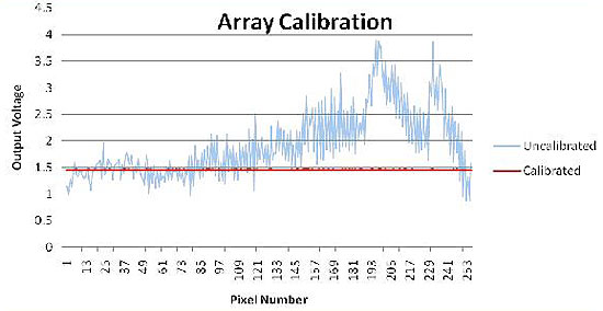
Fig. 1: Effectiveness of Per Pixel Dark Current Subtraction
Environmental Sensitivity
Wet chemically deposited PbS and PbSe photoconductive films are polycrystalline in structure. The materials used in their fabrication produce films that are hygroscopic, sensitive to UV radiation, and mechanically fragile. The film characteristics can also change or be destroyed at high temperature or with condensing moisture.
The solution is to insure that the components are hermetically maintained in an inert environment. Proper selection of the backfill gas can also help with the thermal load presented to the thermoelectric cooler. Vacuum packaging is also an option, but is not required for the reasonable operating temperatures used by lead salt photoconductors and the complexity is usually avoided.
Small Geometries
Single element detectors produced from wet chemically deposited photoconductive films have traditionally been delineated by standard photolithographic techniques. Current array geometries are typically 40 µm x 450 µm for spectroscopic arrays and 40 µm x 40 µm for thermographic arrays, both with inter-element gaps of 10 µm. These geometries are compatible with most infrared optical systems and provide enough photon collection area to produce reasonable signals. Although these geometries do not push the limits of photolithographic techniques, with traditional deposition methods the polycrystalline films and substrate surface finishes the topographies make fine photolithography difficult. In addition the films are sensitive to undercutting which can occur with photolithographic etching and increases the resistance variability in arrays with small geometries.
Ion milling provides a method of delineation with finer detail in these situations(4) and eliminates some of the disadvantages of photolithography.
Implementation
A key to success in producing robust products is the application of proven processes. The balance is between pushing the technical envelope to increase product usefulness and making sure the applied technologies are mature enough to yield consistency and reliability in the end application. This is a second generation implementation that refines the initial work done on lead salt photoconductive arrays implemented only for spectroscopic applications. This second generation implementation enhances the previous design and expands the application base to thermography and thermal imaging with a 40 µm x 40 µm pixel option.
The implementation consists of the following elements that address the stated detector issues:
• A chemically deposited detector array which uses a combination of photolithography and ion milling to produce the required geometries in both rectangular and square pixel configurations.
• A dedicated second generation silicon chip to handle the electronic interface to the array and provide other features and enhancements.
• An industry standard package capable of housing the critical components in a hermetic environment with a UV/Visible filtering window.
• A thermoelectric cooler with physical, thermal and electrical characteristics matched to the package and thermal load.
• A thermal sensing element carefully positioned to provide the optimal feedback to a control circuit.
Figure 2 and Figure 3 show the design concept, which considers all of the aspects of the design. 3-D modelling was important to capture the physical, electrical and thermal aspects of the design. The manufacturability of the design to produce a good cost/performance ratio was also a primary consideration and is shown implemented design is shown in Figure 4. The detector pixels can be either rectangular for spectroscopic applications, or square for thermographic applications. The entire design, including the interface IC, can accommodate either configuration thereby providing a universal solution.
A key component is a second generation readout interface chip (ROIC) which has been developed by ADIC, Inc. (Longwood, Fla ). This chip provides the following features:
• Both global and 8 bit per pixel dark current subtraction
• 4 MHz data readout speed
• Signal integration with selectable charge well size
• Input circuitry specifically designed to interface with PbS and PbSe photoconductors.
• Advanced functionality including:
o Data windowing
o Bidirectional readout
o Read while or after integration
o Single supply operation
Although a seemingly simple component, the lid assembly provides hermetic sealing, UV/Visible blocking for both the silicon chip and detector array with good transmission over the wavelengths of interest, and an optical aperture so careful design and material selection is critical. Figure 5 shows the fully packaged array, including an AR coated silicon window. The geometry of the window is such that the welding fixture provides the alignment necessary to insure that background radiation is rejected while not vignetting the array elements.
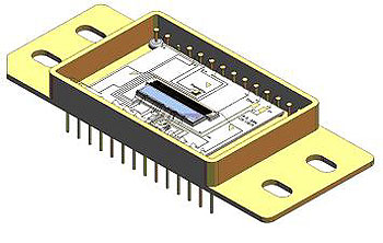
Fig. 2: Design Concept
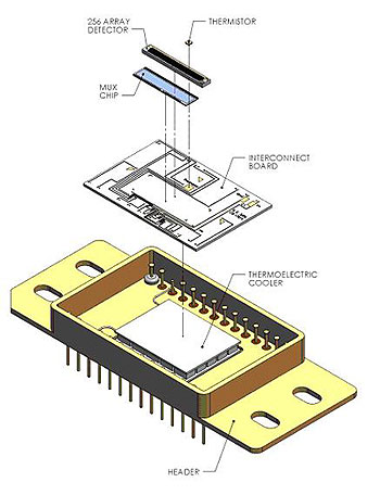
Fig. 3: Design Concept, Exploded
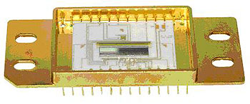
Fig. 4: Design Realized, Internal
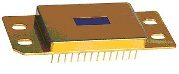
Fig. 5: Design Realization, Packaged
Conclusion
Lead salt photoconductive films are a mature technology that have shown general usefulness as detectors in the near and mid infrared regions in both spectroscopic and thermographic applications. Advances in integrated circuit design, photolithography, ion milling, hermetic sealing and thermoelectric cooling can be applied to produce detector array assemblies that take advantage of the benefits of photoconductive arrays while compensating for their various characteristics. These issues and their solutions have been presented in theory and practice, showing an economically producible detector array package for easy implementation in both spectroscopic and thermographic applications.
For more information, visit: www.calsensors.com
Also See: More Web Exclusives
References
1. Rogalski, Antoni. Infrared Photon Detectors. Bellingham : SPIE, 1995.
2. Woodward, W. Stephen. Thermoelectric-cooler unipolar drive achieves stable temperatures. EDN. 3. December 2007, S. 98.
3. Study of a Silicon Photodetector Thermal Stabilization using a Peltier Cell. E. Foschi, C. Guandalini, G. Levi, L. Quadrani, C. Sbarra, M. Zuffa. Grenoble : Proceedings of the COMSOL Users Conference, 2007.
4. MITTAL, V., et al. Ion beam milling of n-type mercury cadmium telluride for photoconductive devices. SPIE Proceedings. 16. September 1997, S. 799 - 802.