A semiconductor-free, optically-controlled microelectronic device fabricated using metamaterials has shown a significant increase in conductivity when activated by low voltage and a low power laser. The discovery may facilitate the development of microscale electronic devices that are faster and capable of handling more power, and could also lead to more efficient solar panels.

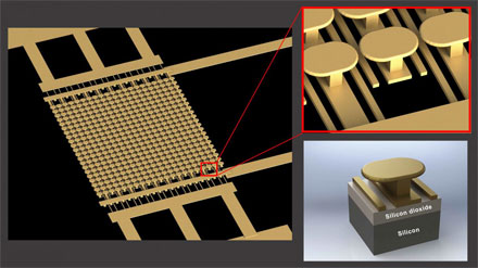
The designed semiconductor-free microelectronic device. Courtesy of UC San Diego Applied Electromagnetics Group.
The device consists of an engineered metasurface on top of a silicon wafer, with a
layer of silicon dioxide in between. The metasurface is made from an
array of gold mushroom-like nanostructures on an array of parallel gold strips.
Researchers at University of California San Diego, who developed the device, showed that the interaction between the device’s metasurface and a low-power IR laser could generate enough photoemission via electron tunnelling to activate microelectronic devices such as transistors, switches and modulators. When a DC voltage of under 10 V and a low power IR laser were applied to the metasurface, “hot spots” with high-intensity electric fields were generated. These hot spots provided enough energy to pull electrons from the metal and liberate them into space.
Tests on the device showed a 1,000 percent increase in conductivity.

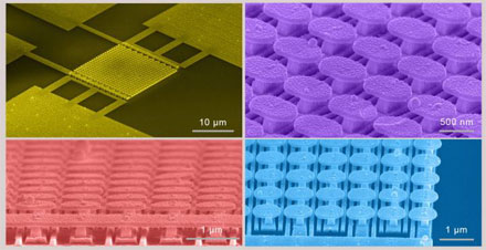
These are scanning electron micrograph images of the semiconductor-free microelectronic device (top left) and the gold metasurface (top right, bottom). Courtesy of UC San Diego Applied Electromagnetics Group.
Replacement of semiconductors with substitute materials may open up new opportunities for scaling characteristics such as speed and power for some applications. As further optimization of semiconductor devices becomes more challenging, photoemission-based devices, which benefit from the advantages of gas-plasma/vacuum electronic devices while preserving the integrability of semiconductor-based devices, may be a feasible option.
"This certainly won't replace all semiconductor devices, but it may be the best approach for certain specialty applications, such as very high frequencies or high power devices," professor Dan Sievenpiper said. "Next we need to understand how far these devices can be scaled and the limits of their performance."
According to researchers, this particular metasurface was designed as a proof-of-concept. Different metasurfaces will need to be designed and optimized for different types of microelectronic devices. The team is also exploring other applications for this technology besides electronics, such as photochemistry, photocatalysis, and enabling new kinds of photovoltaic devices.
The research was published in Nature Communications (doi:10.1038/ncomms13399).
Engineers at the University of California San Diego have fabricated the first semiconductor-free, optically-controlled microelectronic device. Using metamaterials, engineers were able to build a microscale device that shows a 1,000 percent increase in conductivity when activated by low voltage and a low power laser. The discovery paves the way for microelectronic devices that are faster and capable of handling more power, and could also lead to more efficient solar panels. Courtesy of Kindea Labs.