For Samuel P. Sadoulet, one of the most
important trends in optics can’t be seen – literally. As executive vice
president of engineering and manufacturing at Barrington, N.J.-based optical component
provider Edmund Optics, Sadoulet knows what he is talking about.
In this case, the point is that much of the growth in optics will
come outside of what our eyes can register. “Visible optics within industrial
and scientific applications is growing 5 to 10 percent globally, maybe,” he
said. But for IR and UV, it’s much higher than that, he noted. “My guess
is well north of 15 percent.”

To better see the invisible, there is increasing
demand for stock IR optics, such as these zinc selenide IR aspheres for wavelengths
from 0.6 to 18.0 μm. Courtesy of Edmund Optics.
This push into previously somewhat invisible areas is being driven
by technology advances and applications that demand enhanced performance. An example
is the falling price of IR sensors, which is turning a formerly military-oriented
market into one that is more commercial- and price-sensitive. For IR optics, this
means that custom configurations are giving way to lower cost and more standardized
products.
But this trend of venturing into new territory extends to more
than just spectrum. There are new materials and new ways to use materials, such
as plasma mirrors that can generate new laser wavelengths. Another example comes
in the form of glass improvements that could enable the creation of lasers thousands
of times more powerful than anything existing today. There is the use of plasmonics
to enhance sensing, shrink devices or power optical antennas that manipulate light.
There also are advances in fiber optics that promise double (or even higher) data
rates.

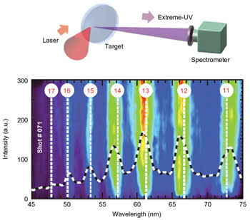
A laser-generated plasma mirror produces high-order harmonics, creating a sub-10-nm
source from an 800-nm central beam. Setup on top yields the eighth to 20th harmonics
on bottom. Reprinted from Applied Physics B. Courtesy of Dr. Laszlo Veisz, Max Planck
Institute for Quantum Optics.
While acknowledging that conventional optics faces cost and performance
pressures, Sadoulet doesn’t see coming advances replacing traditional approaches.
Instead, the new will complement the old, he predicts. “We saw an analogous
story unfold in imaging. The development of software algorithms has not rendered
the optics obsolete. There are certain problems best handled with an algorithmic
solution, and other issues best solved by optics.”
An illustration of new approaches complementing or extending what
can currently be done is found in a plasma mirror. This technique, the subject of
research around the world, translates existing lasers into new spectral areas, making
up for the lack of suitable lasing materials.
In a plasma mirror, a metal or another solid is hit by an intense
femtosecond laser pulse. The beam interacts with the surface, producing a plasma
that reflects the incoming light. The laser also drives the surface in a rapid up
and down oscillation. As a result, the mirror generates harmonics that are much
higher in frequency – and therefore have a much shorter wavelength –
than the original beam.
“You can reach 20, 50, even hundreds of the initial harmonic.
So if you calculate, then you can have an 800-nm initial, and its harmonic is at
or even below 8 nm,” said Csaba Toth, a staff scientist at Lawrence Berkeley
National Laboratory in Berkeley, Calif. He was chairman of the optical sciences
section of the 2010 Frontiers in Optics conference held in Rochester, N.Y., in October.
For researchers, a plasma mirror offers a way to create new light
sources. An example might be an attosecond extreme-ultraviolet or soft x-ray pulse
source, derived from the coherent combination of high-order harmonics of a familiar
Ti:sapphire laser. Such a short wavelength source would be useful for time-resolved
spectroscopy of atoms, molecules and solids.
In practice, producing a plasma mirror from solid targets would
be destructive. The laser would strike the material, creating the plasma and a micron-size
crater. Before the next shot, the target would be moved over a few microns so that
a fresh surface could be used.
There is a clear technology path to get up to repetition rates
of about a kilohertz, Toth said. Beyond that, advances in target quality, replenishment,
preparation and management may be needed.
Target management also is needed for laser-driven particle accelerators.
Either directly or through plasma interactions, a laser of a high enough peak power
can force electrons and protons to an appreciable fraction of the speed of light.
A laser-driven accelerator would be 100 times smaller than those using the traditional
approach, with perhaps a tenfold cost savings over conventional methods, Toth said.
As for applications, these accelerators could produce a proton
beam for cancer treatment, the utility of which has been proved in principle by
studies. Groups in the US, Europe and Japan are working on this, and Toth forecasts
success within five or so years, if a suitable laser is available. To succeed, the
researchers must focus femtosecond pulses down to a small size, achieving power
densities of at least 1018 W/cm2.
That number, 1018 W, is an exawatt, which happens to be the relevant
number for newly launched laser projects. To get an idea of how much power this
is, an exawatt is six orders of magnitude greater than the capacity of the entire
US electrical grid.

An exawatt laser – one thousand times more powerful than current
lasers – is under development. It will use technology from the Texas petawatt
laser, the amplifier chamber shown above, and new materials developed by Schott
North America Inc. Courtesy of the University of Texas.
Schott North America, the Elmsford, N.Y.-based subsidiary of the
German company, has contracts to develop and supply the glass and other optical
materials that will be used in the University of Texas at Austin’s exawatt
project.
A 1000-times-less-powerful petawatt laser based on this idea has
already been demonstrated. It outputs 1057-nm-wavelength, 200-J, 150-fs pulses,
which puts it at >1.3 PW. To pump that up into an exawatt requires, among other
things, new laser glass materials that allow amplification to the higher energy.
This demands basic research into optical materials and how to make them, said Eric
H. Urruti, Schott North America’s director of research and technology development.
“The energy flux is so high, you’re at risk of either
melting the glass or, if there’s any flaws in the glass, causing it to rupture
and explode. So we need to make the glass more robust,” he said.
He expects that it will take about half a decade before this initial
development bears fruit, and the entire exawatt project may not result in a laser
for twice that long. In the meantime, advances in optical fabrication technology
could pay off in other areas.
For example, being able to build optical materials with fewer
internal flaws and greater homogeneity could prove beneficial in imaging. Imperfections
in optical materials degrade an image before it gets to a sensor. More perfect materials
would eliminate this problem, enabling devices to be downsized without sacrificing
performance.
Schott North America has contracts with the US government to devise
ways to produce more homogeneous material, which Urruti said can be done by shifting
the manufacturing process. Pulling this off would benefit all optical applications
because it is likely to result in lowering the cost of the highest grade material.
Another materials-oriented effort shows the push to put plasmonics
to work. This approach exploits the quantized plasma oscillations, or plasmons,
found at the surface of metals that arise from the interaction with light. Plasmonics
alters the optical properties of metals, leading to useful effects.
A case in point comes from research at the University of Dayton
in Ohio by associate professor of electro-optics Qiwen Zhan. He helped design and
demonstrate a plasmonic spiral lens, with 200-nm-wide slots fabricated in a 200-nm-thick
gold film.

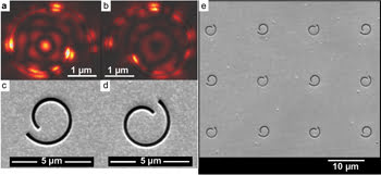
A better spiral lens with plasmonics.
(a) Left-hand spiral plasmonic lens focuses right-hand circular polarization, while
(b) a right-hand spiral plasmonic lens defocuses it, as seen by the lack of a central
bright dot; (c-d) scanning electron micrograph of left- and right-hand spiral lens;
(e) an array of alternating handedness. Courtesy of Qiwen Zhan, University of Dayton.
This approach offers a number of advantages over traditional optics,
Zhan said, including allowing detection of the circular polarization component in
the field of view without the need for a clumsy – and slow – mechanical
rotation of a quarter-wave plate. Being able to collect full polarization data is
useful for surveillance, agriculture, environmental studies and other remote-sensing
applications, he added.
It also enables miniaturization. “The new device will enable
us to remove the bulk polarization devices – polarizer, wave plates, and so
on – and integrate the device directly onto a detector array, such as a focal
plane array or CCD. Thus, the amount of size reduction really depends on how small
one can fabricate the chip.”
He believes that, in the future, optics will increasingly combine
an engineered optical field with engineered materials, such as was done with the
plasmonic spiral lens. This will provide a great deal of freedom in optical design,
fabrication and instrumentation.
One possibility would be a plasmonic transistor, or plasmonster,
said Zhaolin Lu, an assistant professor of microsystems engineering at Rochester
Institute of Technology in New York. Just as a transistor does to electrons, a plasmonster
would allow light to be switched on/off, magnified, diminished or otherwise altered.
One problem with this vision is that metals, the materials of
choice for plasmonics, are not perfect reflectors of light in the optical. Instead,
the light penetrates a few tens of nanometers into the surface of the metal.
“The challenge is that metal is an absorptive medium. So
the absorption is huge for most plasmonic devices,” Lu said.
In another example from plasmonics, it is now possible to build
the optical equivalent of a radio antenna. Such devices, unlike mirrors or lenses
or other traditional optical components, manipulate photons using elements that
are approximately 100 times smaller than the wavelength of light. For an optical
antenna, that puts the relevant dimensions at a few nanometers, a dimensional requirement
that is now within reach of current fabrication technology.
Lukas Novotny, a professor of optics and physics at the University
of Rochester, believes that optical antennas could be used to boost the efficiency
of LEDs and photovoltaics as well as to improve the ability of spectroscopy to detect
minute traces of chemicals because an optical antenna enables a more effective interaction
of light and matter.
The most promising near-term application is photodetection, he
said. An optical antenna would make a photodetector with a small area capture light
as efficiently as one with a much larger area. The smaller detector area would decrease
dark noise, while the optical antenna would mean no sacrifice in the signal. The
combination would therefore increase the signal-to-noise ratio of the detector.
The sensor would be faster and more energy efficient as well.
“Probably all of this will first be approached in the infrared
regime. It’s easier to fabricate,” Novotny said. “I can imagine
for night vision systems this would be a very attractive route to go.”
A key need is for ultrapure, defect-free materials. A group at
the University of Würzburg in Germany recently demonstrated how to grow single-crystal
metal, which is much more uniform than the typical metal, offering a possible solution
to this problem.
Optical antennas and other plasmonic devices could prove useful
in telecommunications. That day, however, is years away.
Telecommunications improvements are needed because data traffic
is growing at 40 to 50 percent a year, said Alan F. Evans, research director for
optical physics and transmission at Corning Inc. in Corning, N.Y., a manufacturer
of fiber, specialty glass and ceramics. Forty years after the initial paper on low-loss
fiber was published, the loss per kilometer of the latest fiber has fallen to 0.16
dB/km, below the longtime standard of 0.19. There also is now the ability to make
larger-diameter fiber with, therefore, less optical nonlinearity.
As a result, systems with the new fiber have more operating margin,
which could benefit future data demands, Evans said. “You can use that system
margin any way you want. One way would be obviously to modulate the signal with
multiple phase or amplitude levels, increasing the information-carrying capacity.”
At the same time, advances in nanofabrication are helping companies
and consumers get the most out of the current crop of optical fiber. At present,
the commercial state of the art for data communications is 100 Gb/s over fiber optic
lines, said Peter J. Winzer, director of optical transmission systems and advanced
networks research at Bell Labs, the Murray Hill, N.J.-based research arm of Alcatel-Lucent.
In June, the company announced availability of what it claimed
as the industry’s first single-wavelength 100-Gb/s solution, made possible
through the use of coherent detection technology. This uses a free running laser
oscillator at the receiver, which beats against the incoming signal. The resulting
interference varies from constructive to destructive and everything in between.
This beating permits detection of the optical field’s amplitude, phase and
polarization, allowing more modulation than possible with a simple on/off scheme.

By going with the beat and coherent detection technology, data rates
of 100 Gb/s – or more – through optic fiber (top) and cable (bottom)
have been achieved. Courtesy of Bell Labs.
Alcatel-Lucent’s single-wavelength solution uses this capability
to pack more information into every symbol transmitted, with as many as 4 bits encoded
into each. However, it requires digitizing the incoming signal at a high speed,
which the company achieved by designing its own custom chip. This was possible only
by exploiting the latest chip technology.
Alcatel-Lucent is already working to extend its bit-cramming technique
and has had some success in the lab, Winzer said. “We’ve demonstrated
two things. We’ve demonstrated more than a doubling in spectral efficiency
at 100 Gb/s. And we have gone all the way to 400 Gb/s.”
The latter is important for future applications because next-generation
Ethernet may have a 400-Gb version. The day that this lab demonstration will be
needed in the field may not be that far off, Winzer said.
With current technology, the terabit level, 10 times today’s
best rate, will demand multiple wavelengths or fibers, he noted. Beyond that, current
fiber technology will hit its effective capacity limit sometime within the next
decade. The solutions under consideration include lower nonlinearity or lower-loss
optical transmission fiber, transmission over extended wavelength ranges, or even
the use of multicore or multimode optical fiber.
It is possible that some new materials and techniques, such as
those based on plasmonics, may prove useful when the time comes to deploy the new
network. What is clear is that, with infrastructure changes involved, it will take
years to roll out. Thus, the required research and development must be done today.
As Winzer said, “You do have to work on radically new fiber
designs now in order to be able to supply the fiber and the system and the management
platform for the network that runs on this new fiber in the 10-plus time horizon.”