Organic photodetectors are destined to enhance numerous sectors ranging from industrial markets for process control, object recognition and light management to consumer electronics for motion detection and interactive surface applications.
OPDs, also known as organic photodetectors, have a lot going for them: They can be lightweight, thin, flexible, semitransparent and cheap to make, and they can be manufactured in large sizes. Currently, OPDs are still in the product development stage, but in the coming years, they will make their way into many types of products and applications, thanks to the unique properties that set them apart from traditional electronics.
The first distinction between OPDs and their traditional photodetector counterparts is that they are based on carbon rather than silicon. The organic conductor and semiconductor materials that make up OPDs were originally developed by organic chemistry giants and material startup companies for the organic photovoltaics market.
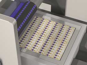
A screen printing process for printed electronics is illustrated. Courtesy of CEA LITEN.
Second, the manufacturing process is totally different from the one used for the conventional photodetector, which requires vacuum deposition at high temperatures. OPDs, on the other hand, can be printed at ambient temperatures using high-throughput, large-area processes such as screen printing, gravure printing and spray coating.
Finally, OPDs can be assembled on glass or plastic substrates. The flexibility of the latter opens the door to new uses and places for OPDs, such as in tubes.
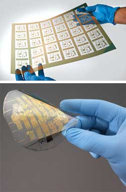
Top and bottom left: Organic photodetectors printed on plastic foil. Courtesy of CEA LITEN.
This new technology is attracting more and more interest from groups in the pharmaceutical, energy and environmental industries, giving them opportunities for product creation with easier mechanical integration and novel functionalities. For example, large-area sensors are useful for monitoring phenomena such as liquid analysis and motion scanning, without the additional optics that conventional photo-detectors require for image focus.
Qualities critical to their performance include high frequency response and high sensitivity; however, today’s OPDs have high sensitivity but a rather low frequency response. Serious research activity is under way to bring together the right organic materials in just the right way to optimize the OPD’s most prized characteristics.
The anatomy of the OPD is based on a photodiode device structure that converts incident light or photons into information or an electric current. A high external quantum efficiency, or conversion ratio of incident photons to current, is obtained by blending two organic semiconductors, a p type and an n type, sandwiched between two electrodes. Excitons generated by photons are separated into electrons and holes to create an electric current that can be measured for signal processing.
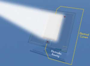
Light conversion by organic photodetector under voltage bias. Courtesy of ISORG.
A promising class of materials that has emerged in the past decade includes fullerene derivatives, which are expected to exhibit relatively high photoelectric conversion efficiency under applied voltage.
Fullerene derivatives doped in several conducting polymers act as an effective quencher and electron accepter, researchers have discovered. Katsumi Yoshino et al at Osaka University in Japan and Alan J. Heeger and colleagues at the University of California, Santa Barbara, found that the photophysics characteristics of fullerene derivatives exhibit ultrafast photoinduced charge transfer.
At Osaka University, Yutaka Ohmori and Hirotake Kajii in the graduate school of engineering have spent several years investigating high-speed OPDs based on fluorene-type polymers. These polymers can be selected by absorption wavelength, making color-sensitive photodetectors a reality.
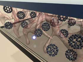
A bulk heterojunction organic photodetector device structure is illustrated. Courtesy of ISORG.
Fluorene-type polymers also have ambipolar characteristics, high stabilities and relatively high mobilities, which make them promising materials for large-area OPDs. On the other hand, fullerene derivatives also have relatively high electron mobilities. The photogenerated excitons are easy to dissociate at the conjugated polymer:fullerene derivative bulk heterojunctions.
High-speed response of printable OPDs has been reported by Ohmori and colleagues. The group found that pulsed signals of approximately 100 MHz have been received by OPDs fabricated by the solution process. Printable OPDs have potential in micro-optics of photodiode arrays.
For Laurent Jamet – co-founder and business development director of ISORG, an organic and printed electronics company based in Grenoble, France – the most significant advance in OPD technology results from the availability of materials that do not degrade due to oxygen or water. These stable materials allow for robust manufacturing processes and result in products that withstand the test of time.

The ISORG Magic Pad 3-D multimedia interactive tablet uses OPDs to detect motion in three dimensions. OPDs are still in product development but likely will appear in various products and applications in the years to come. Courtesy of ISORG.
ISORG is working on innovative uses for OPDs, including a device it calls the Magic Pad, which enables a 3-D user interface that is generally noncontact. The Magic Pad comprises a matrix of OPDs, housed in a plastic cover, that can recognize motion, speed and hand position.
“We have developed a functional demonstrator called the Magic Pad which demonstrates capability to interact with a plastic or glass surface without any contact in three dimensions for different applications: gaming, entertainment, multimedia, industrial display,” Jamet said. “Most of the functionalities of Magic Pad are operated without any contact; this is the ‘magic’ effect of this demonstrator.”
Other possible applications lie in consumer products such as home appliances, user interfaces for consumer electronics, ambient light sensors and toys, as well as interactive printed media and smart packaging.
At this stage, the Magic Pad is solely a demonstrator tool, but ISORG is in discussions with various companies for product concepts; Jamet expects that the first products derived from this model will appear within a couple of years.
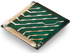
A matrix of organic photodetectors on glass. Courtesy of CEA LITEN.
Photovoltaic research could benefit OPDs
In 2020, the market for sensors in printed electronics will be around $2.2 billion, according to an estimate from IDTechEx, a market analysis and consulting firm in Cambridge, Mass., that covers printed electronics.
Of this market, Jamet believes that OPDs will represent a significant proportion, with the biggest user in the long term likely to be found in the consumer electronics industry. Here we could see OPDs integrated into television displays and e-tablets, for example.
In the shorter term, Jamet predicts that the next breakthroughs will be in new materials that can operate over a larger spectrum. “Today, our photodetectors are operating in the visible and near-infrared spectrum (400 to 1000 nm),” he said. “There is strong interest from the market to go up to 1400 to 1500 nm.”
With this in mind, research and development teams are looking to develop new materials with inorganic nanoparticles such as quantum dots mixed with polymers to extend the spectrum operation.
“Other R&D activity is to develop transparent electrodes – based, for instance, on carbon nanotubes – for easier photodetector integration in display or smart building markets,” Jamet said.
Fabricating transparent electrodes for organic solar cells is currently a hot research topic. Because OPDs and photovoltaics have the common functionality of transforming light into electrical current, any progress in the photovoltaics field could benefit the OPD market.
For example, scientists at the University of Warwick in the UK recently found that extremely thin gold plates could be deposited on transparent electrodes for organic solar cells (see “Solar cell electrodes could turn market to gold” on p. 41 of the June issue).
Molecular Solar, the commercializing force behind the university’s endeavors in solar cell development, believes that gold is the ideal material to replace the traditional indium tin oxide (ITO) for electrode coating and that gold may enable mass production on flexible substrates.
The trouble with ITO is that it is a complex, unstable material with a high surface roughness and a tendency to crack upon bending when supported on a plastic substrate. If that weren’t bad enough, one of its key components, indium, currently is in short supply, making it relatively expensive to use.
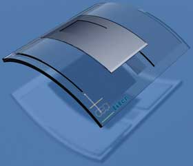
Concept of flexible photodetector on plastic. Courtesy of ISORG.
Other groups have looked at silver nanowires as a possible candidate to replace ITO. Researchers at the Henry Samueli School of Engineering and Applied Science at the University of California, Los Angeles, claim that their new electrode uses low-cost, nontoxic and stable materials and is easy to fabricate. Silver nanowires are produced on a cross-linked, transparent polyacrylate substrate that is more economical than glass and can be either stiff and rigid, or flexible and stretchable.
Yet another material that could help make solar cells inexpensive, lightweight and flexible is graphene. A team at MIT in Cambridge reports that graphene-based electrodes could open up a variety of applications that would not be possible with today’s conventional silicon-based solar panels. For example, because of their transparency, they could be applied directly to windows without blocking the view, or to irregular wall or rooftop surfaces.
But translating research carried out with photovoltaics in mind into material benefits in OPD systems will require some re-engineering, as Jamet explains.
“OPDs require a linear response versus the received light. They also require a low dark current – i.e., current which is generated with low illumination – to have a wide current range when in light and in dark conditions,” he said. “We are also looking for operation in the near-infrared (starting at 900 nm), whereas photovoltaics operates only in visible (400 to 700 to 800 nm).”