New Lithography Method Creates Molecule-Sized Images
EVANSTON, Ill., Sept. 29, 2006 -- Ever since the invention of the first scanning probe microscope in 1981, researchers have believed the powerful tool would someday be used for the nanofabrication and nanopatterning of surfaces in a molecule-by-molecule, bottom-up fashion. Despite 25 years of research in this area, scientists had hit a brick wall in developing a technique with commercial potential -- until now.
Northwestern University researchers have developed a 55,000-pen, two-dimensional array that allows them to simultaneously create 55,000 identical patterns drawn with tiny dots of molecular ink on substrates of gold or glass, with each structure being only a single molecule tall. This advance of a patterning method called dip-pen nanolithography (DPN), which was invented at Northwestern in 1999, was published online Monday by the journal Angewandte Chemie.

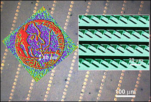
The background shows some of the 55,000 miniature images of a 2005 US nickel made with dip-pen lithography. (Each circle is only twice the diameter of a red blood cell.) Each nickel image with Thomas Jefferson's profile (in red) is made of a series of 80-nm dots. The inset (right) is an electron microscope image of a portion of the 55,000-pen array.
To demonstrate the technique's power, the researchers reproduced the face of Thomas Jefferson from a five-cent coin 55,000 times, which took 30 minutes. Each identical nickel image is 12 µm wide -- about twice the diameter of a red blood cell -- and is made up of 8773 dots, each 80 nm in diameter.
The parallel process paves the way for making DPN competitive with other optical and stamping lithographic methods used for patterning large areas on metal and semiconductor substrates, including silicon wafers. The advantage of DPN, which is a maskless lithography, is that it can be used to deliver many different types of inks simultaneously to a surface in any configuration one desires. Mask-based lithographies and stamping protocols are extremely limited in this regard.
"This development should lead to massively miniaturized gene chips, combinatorial libraries for screening pharmaceutically active materials and new ways of fabricating and integrating nanoscale or even molecular-scale components for electronics and computers," said Chad A. Mirkin, director of Northwestern's International Institute for Nanotechnology and George B. Rathmann Professor of Chemistry, who led the research.
"In addition, it could lead to new ways of studying biological systems at the single particle level, which is important for understanding how cancer cells and viruses work and for getting them to stop what they do," he said. "Essentially one can build an entire gene or protein chip that fits underneath a single cell."
In addition to Mirkin, other authors on the paper are Khalid Salaita (lead author), Yuhuang Wang and Rafael A. Vega from Northwestern; Joseph Fragala from NanoInk, Inc.; and Chang Liu of the University of Illinois at Urbana-Champaign.
The research was supported by the National Institutes of Health, DARPA, the Air Force Office of Scientific Research and the National Science Foundation. For more information, visit: www.northwestern.edu
Published: September 2006