A nanophotonic cladding cloak that prevents crosstalk between two closely spaced single-mode waveguides could allow photonic devices to be integrated at a much higher density, without causing light to leak from one waveguide to another. This would allow billions of photonic devices to be packed into a single photonic computer chip and reduce the footprint of the chip, overcoming a major obstacle to the use of photonic chips in computers, data centers and mobile devices.
Researchers at the University of Utah placed a nanopatterned silicon-based barrier between two photonics devices to render neighboring devices invisible to one another. An inverse-design algorithm was employed to design an integrated cloak with a footprint of just a few micrometers.
Experimental results demonstrated that waveguides with a center-to-center spacing as small as 0.8 μm (λ0/1.94) were feasible. This could potentially double the integration density of planar lightwave circuits (PLCs), as the conventional minimum center-to-center spacing between parallel waveguides is about 1.5 μm.
The nanophotonic cloak also prevents crosstalk between a single-mode waveguide and a closely spaced micro-ring resonator. This device configuration is commonly used for filters, and such cloaks could be useful for integrating multiple filters into a small area.

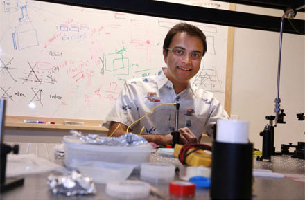
University of Utah electrical and computer engineering associate professor Rajesh Menon and his team have developed a cloaking device for microscopic photonic integrated devices — the building blocks of photonic computer chips that run on light instead of electrical current -- in an effort to make future chips smaller, faster and consume much less power. Courtesy of Dan Hixson/University of Utah College of Engineering.
"The principle we are using is similar to that of the Harry Potter invisibility cloak," said professor Rajesh Menon. "Any light that comes to one device is redirected back as if to mimic the situation of not having a neighboring device. It's like a barrier — it pushes the light back into the original device. It is being fooled into thinking there is nothing on the other side."
The devices used in the research are metal-oxide-semiconductor compatible, with a minimum pitch of 200 nm; and can be fabricated with a single lithography step. The nanophotonic cloaks can potentially be used with all passive integrated photonics.
Menon believes the most immediate application for this technology and for photonic chips in general will be for data centers similar to the ones used by services like Google and Facebook. According to a study from the U.S. Department of Energy's Lawrence Berkeley National Laboratory, data centers just in the U.S. consumed 70 billion kW hours in 2014, or about 1.8 percent of total U.S. electricity consumption. Power usage is expected to rise another 4 percent by 2020. Photonic chips consume 10 to 100 times less power and give off significantly less heat than silicon-based chips, and are also faster than silicon-based chips.
"By going from electronics to photonics we can make computers much more efficient and ultimately make a big impact on carbon emissions and energy usage for all kinds of things," Menon said. "It's a big impact and a lot of people are trying to solve it."
Currently, photonic devices are used mostly in high-end military equipment. Menon expects full photonic-based chips will be employed in data centers within a few years.
The research was published in Nature Communications (doi: 10.1038/ncomms13126).