Advanced microscopy techniques have been used to show that adding the optimum amount of selenium (Se) may help increase efficiency in cadium (Cd)- and tellurium (Te)-based solar cells from the current approximate 22 percent to levels approaching the theoretical limit of 30 to 33 percent.
To study the effect of Se content on the photoactive properties of bandgap-graded CdTe cells, researchers at Oak Ridge National Laboratory (ORNL) used a combination of techniques including atom probe tomography, transmission electron microscopy and electron beam-induced current.

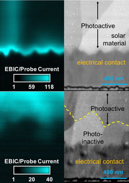
The entire solar material for the sample with less than or equal to 30 percent selenium is photoactive (top), while the bottom of the solar material for the image below contains greater than 35 percent selenium and has reduced photoactivity. Courtesy of ORNL.
"Using different microscopy methods, we were able to gain a better understanding of the phases, compositions and crystalline structures that allow these materials to convert light into electricity more efficiently," said team leader Jonathan Poplawsky. "In some instances, adding too much selenium changes the crystalline structure of cadmium-tellurium and dramatically reduces the conversion efficiency."
The research team studied four solar cells with contents of 50-, 100-, 200- and 400-nm-thick cadmium selenium (CdSe) layers to determine the formation, growth, composition, structure and photoactivity of the CdTexSe1−x alloy with respect to Se diffusion. The carrier separation properties of the cells prepared with the varied CdSe layer thicknesses were measured with 30- to 50-nm resolution using scanning electron microscopy (SEM)-based electron beam-induced current (EBIC), while the crystallography and Se concentration were measured at the nanoscale using transmission electron microscopy selected area diffraction (TEM-SAD) and atom probe tomography (APT), respectively. The results showed an interdependence between the layer’s ability to convert photons into electricity and the Se content and crystalline structure of the layer.

The cell with the alloy composition of approximately 50 percent Cd, 25 percent Te and 25 percent Se performed best. The cell with the highest level of Se did not perform well; nor did the cell with the lowest Se content.
"We have shown that the amount of selenium incorporated into the cadmium-tellurium controls whether the small crystals inside the solar cell form as crystal structure A or crystal structure B," Poplawsky said. "This information can be used as a roadmap for solar cell producers to make improved cadmium-tellurium solar cells that use selenium additions, and hopefully increase the overall efficiency."
Poplawsky noted that solar panels typically use silicon as the material for converting sunlight into electricity. CdTe can absorb the same amount of sunlight as silicon using 98 percent less semiconducting material, thus reducing the overall cost of the solar panel. The ability to increase the power conversion efficiency (PCE) of CdTe-based solar modules without increasing the production costs will make solar power generation more competitive with fossil fuels.
The research was published in Nature Communications (doi:10.1038/ncomms12537).