Dr. William Henry, InfiniLED
A brush with the second law of thermodynamics can increase a product’s on-shelf appeal – and more.
The drive toward LED-based lighting has resulted in the development of devices with ever-increasing light output and color performance. The lumen-per-dollar total is now the figure of merit often used to judge competing LEDs. To enable market uptake, the focus has shifted from efficiency to cost. However, other applications based on LEDs are striving for smaller sizes and more efficient solutions – such as thinner screens or more portable detection systems. These markets are viewed as niches compared with the massive general-lighting applications, but these power-efficient applications are very large in their own right and require technologies that are optimized for their continuing innovation.
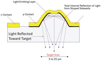
The microLED has been developed to provide a new type of light source for a range of low-power applications. It is built using standard LED materials and therefore has the spectral profile, flexibility and reliability of a standard LED. The microLED offers high efficiency as well as a unique light-controlling structure integrated onto the device during fabrication that results in collimation similar to that of a laser. The design of a microLED is shown in Figure 1. A parabolic structure is created around the light-generation layer of the device. This structure controls the emitted light at the site of light generation and is far more efficient than using external optics after the light has escaped the chip.

Figure 1. This microLED cross section shows total internal reflection leading to high extraction efficiency through a single surface.
In the design and fabrication of LEDs, the difference between the refractive index of the GaN material and that of air is a significant barrier to high-extraction light efficiency. In contrast to standard components, the microLED device uses this fundamental property of the material to enhance performance. Total internal reflection from the sidewalls of the parabolic structure within the microLED focuses the light toward the extraction surface; the design and shape of the sidewalls are accurately controlled to ensure that a high proportion of the light reaches the exit surface perpendicular to the interface. This results in minimal backreflections, high light-extraction efficiency and good control of the beam shape.
In addition, the majority of light is extracted through a single surface of the device, which simplifies the design of any optical system. The microLED parabola results in high light-extraction efficiency – with greater than 30 percent of the generated light extracted just through this one surface. This has been shown to be four times higher than the light extracted through a single surface in a standard LED chip, thereby increasing the amount of usable light within a system. The control and collimation at source are also hugely important for array applications where the light from individual pixels must be distinguishable (i.e., no optical crosstalk).
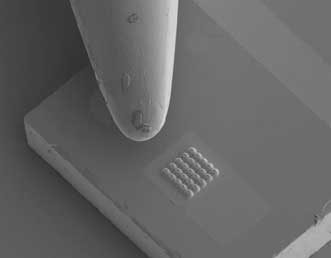
The active area in a single microLED pixel is less than 80 µm2, and the diameter is less than 10 µm. In comparison, a standard LED of dimensions 280 × 280 µm2 will have an active area almost 1000 times greater than that of the microLED. Therefore, to a first approximation, a standard LED requires 1000 times more current to reach the threshold for generating light. Figure 2 shows a cluster of 25 microLED emitters beside the tip of a needle. The quality of the starter material is also a vital factor in the generation of current at low currents: The presence of threading dislocations has been shown to be the source of parasitic losses, resulting in an increase in the current required before light generation. These dislocations are randomly scattered throughout the wafer but are relatively localized at the chip level. In a standard LED, the light is generated over the total area, and, therefore, all the dislocations are seen to affect the performance. However, in the microLED, only a small fraction of the active area is illuminated. In chips where the dislocations are not localized within the active area, the material acts as ultrahigh-quality epitaxial material. This further boosts the performance of the microLED.

Figure 2. A cluster of 25 microLEDs beside the tip of a needle.
The confinement of the light generated is very important for ultralow-power applications – especially when the human eye is the target. The eye is better able to perceive light that is localized over a small area, which reduces the power requirements. A number of techniques have been developed to overcome backreflections and trapping losses for LEDs, primarily around surface roughening. Roughening the exit surface can indeed increase the amount of light escaping, but it results in multiple internal reflections and uncontrolled light being emitted in all directions. Therefore, even when a small emission area is used, it is effective for high extraction and localization of the light only when combined with collimation.
The microLED has been shown to generate light at a drive current of 5 nanoamps (nA). In a darkroom, it can be perceived with the human eye at only 10 nA. Standard LEDs do not generally begin to produce visible light until 100 µA – i.e., 20,000 times more. The power consumption from a microLED is so low that it could produce visible light for up to 80 years using a coin battery. Although 80 years is longer than the active life of a standard battery, the performance of the microLED allows it to be partnered with unique power sources; examples include batteries using new materials, inductive power sources and energy harvesting. Inductive power sources can generate greater than 50 µW of power – more than 100 times the light required to make the microLED visible.
All LED-type devices have an inherent voltage requirement before light is generated. This is well-defined by the bandgap inside the semiconductor and by the magnitude of the transition required to produce light at the defined wavelength. The microLED device has been shown to generate light voltages below this bandgap limit – i.e., the light is more energetic than voltage drop across the source. Thankfully, the microLED does not render the first law of thermodynamics obsolete. At room temperature, a proportion of the electrons are excited above their base state. This reduces the size of the transition required to produce light at the wavelength of interest, so the voltage required to cause a transition and generate light is reduced. This reduction essentially is caused by the microLED device’s harvesting energy from the surrounding environment. This performance is noticeable due to its inherent efficiency at generating detectable light at ultralow-drive conditions. At higher currents, this effect disappears due to the low proportion of electrons in the higher-energy states.
Ultralow-power microLED devices have a broad range of applications. Any device that uses light while being battery-powered can benefit from the power savings. In rangefinding devices, an image is generally formed by placing a mask over a standard LED device. The microLED structure can be customized to remove the need for masking (a significant source of loss) and to simplify the system. When this configuration is coupled with the core efficiency of the devices at low currents, the result can be a greater-than-two-hundredfold improvement in battery life. The low switch-on currents allow the microLED to be coupled with novel power sources, such as induction or energy harvesting.
This enables the use of LEDs in applications that do not have indicators up to this point. One such application could be to provide a visual indicator for security or proof of authenticity. For example, a microLED could be placed on a pharmaceutical packet and coupled with a low-power source. The microLED would be the only light source capable of generating visible light at the ultralow-power levels as a distinguishing property for proof of authenticity. The complexity and cost of equipment required to fabricate an LED would be significant barriers to any attempt to produce unauthorized devices for use on counterfeit products.

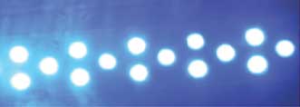
Figure 3. An array of microLED pixels illuminated in parallel.
In a similar fashion, the microLED could be used as a marketing or promotional tool to improve the shelf appeal or brand attractiveness of a product. It could also be used in sensors when the amount of available power is restricted or when high detection sensitivity is required. The devices generate virtually no heat when used in ultralow-power applications. When coupled with their collimation (i.e., a reduced need for optical components), the devices are ideal for both on-body and in-body sensors.
In addition, microLED emitters can be fabricated in arrays and clusters of devices. The cluster – a group of the devices running in parallel – can help build redundancy into the system so that the death of a single pixel will not keep the device from performing. The arrays allow light to come from multiple points that are very close together – but still remain distinct. Figure 3 shows an image of an array of microLEDs as viewed through the device substrate. The arrays can enable low-power displays where the microLED pixels are both the light source and the image engine. Again, the efficiency and simplified optics enable lower-cost systems with longer lifetimes.
Meet the author
Dr. William Henry is chief commercial officer at InfiniLED in Cork, Ireland; email: [email protected].