Dr. William Henry, InfiniLED
Although relatively new, these arrays already are being commercially exploited and have the potential to benefit lighting, lithography, research and other areas.
LEDs are now ubiquitous in everyday life. Deployed initially as infrared communication devices, LEDs now are used as visual indicators, in displays and even for general lighting. However, although the use of LEDs in applications over wide areas has been a long-sought goal, only now are they being extensively exploited to illuminate very small areas.
This new field of LED-based miniature light sources and arrays has been driven by the development of microLED emitters in UV, blue and green wavelengths. These array devices, which are individually addressable, can provide light intensities higher than 300 W/cm2 and can couple light efficiently into areas as small as 50 µm2. Two-dimensional arrays of miniature emitters with pitches as low as 15 µm have been demonstrated. In addition, linear (or 1-D) arrays of emitters with no spacing between pixels have been developed. These arrays enable a range of new applications for LEDs.
LED macro arrays
The most familiar example of addressable LED arrays is in display applications such as those seen on roadside signage or at transportation hubs. These arrays primarily use LEDs because of their power efficiency and low costs. The emergence of blue and green LEDs based on gallium nitride in the 1990s – and their subsequent price reductions – now allow for full-color LED-based displays. A most impressive example can be seen at the Charlotte Motor Speedway in Concord, N.C. This display measures 16,000 sq ft – with proportions of 200 by 80 ft – and contains over 9 million LEDs.
The continued price reduction of LED chips has led to the development of television displays based on direct projection using arrays of three-color LEDs. The high efficiency, contrast and color quality of such direct-image LED displays result in excellent performance, although the products remain more expensive than traditional backlit LCD displays. These big displays might be impressive, but there remains significant room for innovation and interest in arrays at far smaller scales.
Light sources and arrays
In standard LED arrays, each pixel is an individual and unique LED chip. MicroLED arrays, on the other hand, can be fabricated with multiple individual pixels per LED chip. This results in the ability to produce very high pixel densities, intensities and control within a very small area. The challenge is then to make electrical contact to the individual pixels, to control the light generated from each small source, and to ensure that there is no optical crosstalk between the neighboring pixels on the LED chip.
MicroLED (aka µLED) technology from InfiniLED overcomes these issues by bringing together the benefits of LEDs and lasers. The MicroLED has high light intensity and a quasicollimated beam similar to a laser’s. It also allows for the wide wavelength range, temperature stability and flexibility of an LED. To achieve this, a parabolic structure is integrated directly around the site of light generation (Figure 1) by etching the gallium nitride material. The integration of this reflector creates the closest position that an optical component can have to the light-emitting layer. It results in control of the emitted light directly at the source.
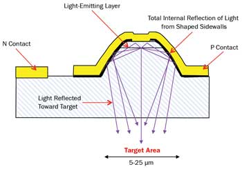
Figure 1. The structure of a µLED with integrated parabolic reflector, which results in high light intensity, a quasicollimated beam, a wide wavelength range, temperature stability and flexibility.
A standard single microLED pixel is typically 20 µm in diameter; Figure 2 shows a cluster of 25 emitters next to the head of a needle. Devices can be fabricated as single pixels, as a large cluster – creating collimated emitters up to 1 mm in diameter – or as arrays of individually addressable emitters. A single pixel can generate up to 1 mW, which results in a light intensity of more than 300 W/cm2. Higher power can be achieved by using clusters of emitters. Arrays are available as both 1-D (i.e., linear) and 2-D addressable formats. Both array types enable a number of applications.
The optics-on-a-chip structure results in a range of performance advantages. The emission angle from the chip is 4x improved over a standard LED (half-angle of 60° vs. 15°). The control of light generated is essential for the fabrication of high-density arrays. The Lambertian emission from a standard LED structure results in overlap between the light produced by pixels. Masking or secondary optics is required to minimize this for standard LEDs, which increases the cost of the device and reduces the amount of usable light. However, the collimated emission from the new µLED minimizes the crosstalk and simplifies the optical system.
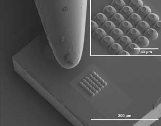
Figure 2. Cluster of 25 µLED emitters beside the head of a needle. Inset: Close-up of microLED emitters showing parabolic reflector structure.
The parabolic structure also greatly increases the amount of light extracted. Figure 3 compares the light extracted from
a µLED to that of a similar planar structure. It can be seen here that 4x more light is extracted from the LED due to the parabolic structure. Only the light that exits from a single face of the semiconductor is measured in this experiment. The test and measurement of standard LEDs involves the capture of light escaping through all six surfaces on the device. However, in µLED array applications, the light that exits from the sides of the chip does not differ significantly from pixel to pixel. Therefore, only the light emitted through the bottom surface of the device is useful.
The ability to produce more usable light results in the µLED using less current than a standard LED to produce the equivalent light. This results in not only power savings (extended life for battery-powered applications), but also lower heat generation.
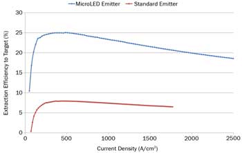
Figure 3. Comparison of light extraction by a µLED versus a planar device. Four times more light is extracted from the LED due to the parabolic structure.
The high extraction efficiency and collimated beam work together to produce an ultrahigh light density. As noted above, more than 300 W/cm2 has been generated by a single µLED pixel. As this light is generated within a narrow set of angles, it can be efficiently captured by the optical system, resulting in very high overall optical system efficiency. Users of these designs have reported a 20x improvement in optical throughput compared with standard, unshaped LEDs.
1-D µLED arrays
Linear µLED arrays can be produced in wide formats of 80 cm and more. In the other dimension, the image area is as small as 5 µm. Red LED arrays have already been applied in printing applications; these arrays have been deployed in both desktop printing and the high-end commercial devices. The addition of the µLED structure to produce collimated beams directly from the chip can result in significant simplification of the optical systems required for printheads. These benefits are relevant in both consumer and commercial printing markets.
The development of blue, green and UV µLED arrays in a linear format also enables significant advantages in existing applications such as lithography and 3-D printing. Long linear arrays can be fabricated, which allows the printhead to be held in position and the target medium to be moved in one direction relative to it. This is particularly important for high-resolution imaging where the optical system is complex and difficult to move. The collimated emission from the µLED has a number of additional benefits, including a simpler optical system, lower power requirements and increased speed.
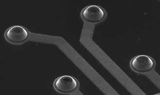
Figure 4. Individually addressable µLED emitters with tracking for contacts.
For lithography applications, a UV LED printhead can be used to image directly on a photosensitive plate. The LED array acts as both the light source and the image engine; it removes the need for masks or other image generators. Due to the high intensities available from the µLED arrays, this maskless lithography technique is faster than current mask-based lithography approaches for the fabrication of PCBs and other materials.
A similar application is the use of µLED arrays for stereolithography apparatus (SLA). Current SLA-type devices use a laser with a moving mirror (laminated sheet, light polymerization and sintering techniques) or 3-D moving head (ink-jet or extrusion techniques). Laser techniques based on movable mirrors required a large depth of field and hence a complicated optical setup. The techniques that require 3-D movement are slower than the optical methods. In contrast, the µLED print-head enables increased accuracy, increased speed and a simplified optical system. In a similar way, this technique can be used in other applications such as DNA synthesis, drug screening and structural (i.e., 3-D) scanning.
2-D µLED arrays
2-D µLED arrays enable a number of exciting new applications. The availability of a range of wavelengths coupled with the ability to control light over a very small area is being exploited in areas such as medical devices, optical stimulation of nerves (optogenetics), maskless lithography, structured light microscopy and microdisplays.
Currently, µLED stimulators for optogenetics are being used primarily in research environments. However, the devices are currently being optimized for implantable use, which will allow them to be used in real-life applications such as cochlear implants, prosthetic eyes or pain treatments.
In microdisplays, the µLED array directly generates the required pattern – with red, green and blue patterns overlapping to produce the image. Since separate imaging (as with a digital micromirror device) is not required, the final device is small, lightweight and efficient. The arrays also show significant promise for high-throughput screening, vision and other applications.
Packaging of µLED arrays
The arrays are available in both matrix and individually addressable formats. Individually addressable arrays present a number of significant packaging challenges. For example, while a 64 x 64 matrix-controlled array requires a minimum of 128 connections, in an individually addressable format, a minimum of 4096 connections is needed. Importantly, the 2-D arrays can be packaged directly on CMOS controllers. This enables individually addressable array modules to be packaged with a reduced number of inputs and a miniature footprint. This is particularly important for portable or implantable applications where space and weight are a concern. The µLEDs are fabricated side by side on the wafer, so their performance characteristics are generally very similar. However, depending on the application tolerances, some calibration may be required. This is carried out as part of the final testing stage.
The majority of µLED arrays are packaged in a flip-chip design (example in Figure 5). This method removes the need for wire bonds and simplifies the packaging process. The light-generating area is also near to a heat sink material, so any heat generated can be quickly removed from the LEDs, which results in minimal heat-induced performance drift.
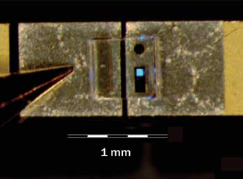
Figure 5. Flip-chipped cluster of 25 µLEDs emitting light toward the viewer. Note the localization of the light generated.
MicroLED devices are fabricated using the same gallium nitride starter material as a large number of standard devices. This allows them to have drive characteristics similar to those of standard LEDs. The light output power can be varied using pulse width modulation or current-limiting techniques. The switch-on voltage is similar to that of other LEDs, although measurable light can be produced at current in the nanoamp range. This is due to the small illumination area and the efficiency of extraction of the light generated. Thermal stability of the µLEDs is similar to that of standard chips. The µLEDs also benefit from the same economies of scale where large volumes are required.
Competing technologies
A number of technologies could be seen as competitors to µLED arrays. Standard LEDs can be arranged in arrays. These can be coupled with high-performance optics to reduce the image size and provide addressability over a small area. However, the starting pixel size is approximately 0.3 x 0.3 mm, and expensive optical components are required to project images onto small areas. In addition, the power available to the system is limited by the size and the emission angle from the chip. The relatively large size of the chip, coupled with its Lambertian emission profile, results in very low light intensity at the target.
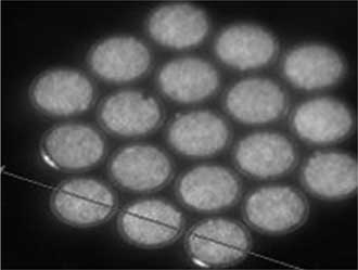
Figure 6. Light from µLEDs is imaged coming through the bottom surface of the device.
Semiconductor lasers in the form of vertical-cavity surface-emitting lasers or edge emitters can also be arranged in arrays. Although arrays up to 16 × 16 have been demonstrated and very high spotlight intensities are possible, the common limitations of semiconductor lasers persist: The primary drawback is the limited wavelength range – with few devices available outside of the red and infrared bands. In addition, array sizes greater than 16 x 16 for 2-D arrays and 24 emitters for linear arrays are not commercially available. Resonant cavity LEDs can also be fabricated as arrays. However, they too are limited by the wavelengths and array sizes available.
Therefore, when it comes to applications requiring high light intensity, addressability and a range of wavelengths, as well as wide-ranging performance stability, the µLED technology proves to be the best-performing and most flexible technology option.
Meet the author
Dr. William Henry is chief commercial officer at InfiniLED in Cork, Ireland; email: [email protected].