Explosive growth in the backlighting market for televisions, displays, handheld devices and more is creating a ripple effect throughout the LED industry. LEDs are sought after for backlighting because of their proven performance, low power consumption, slim form factors, variety of colors and because, unlike fluorescents, they contain no mercury.
According to the September 2009 Quarterly LED & CCFL Backlight Report by DisplaySearch of Austin, Texas, shipments of LED backlight panels grew 116 percent from first- to second-quarter 2009. In a subsequent report, DisplaySearch forecast that fluorescent lighting for notebook PCs, monitors and TV displays would drop to 44 percent in 2011, while LEDs would hold 56 percent of that market.
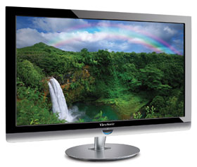
Although Samsung dominated the LED TV market in 2009, according to Displaybank of Bundang, South Korea, announcements at the Consumer & Electronics Show in Las Vegas in January indicate that LED backlit TVs are proliferating and are being marketed not only by many leading manufacturers but also by some who are sidestepping from other lines. ViewSonic, Westinghouse and Haier are just a few of the many who were showing LED-backlit TVs.

New LED-backlit TVs announced at the Consumer & Electronics Show in Las Vegas in January, including this ViewSonic LED HDTV, show that the technology is catching on. Courtesy of ViewSonic.
The good news for LED manufacturers is that they are going to be kept extremely busy into the foreseeable future. Even better news is that many TV makers, such as Samsung, LG and Sharp, are making their own LEDs using metallorganic chemical vapor deposition (MOCVD) process systems.
LED manufacturing
At its core, LED manufacturing is the same as that for producing compound semiconductors: It uses epitaxy, a process in which very thin layers of material are deposited or grown on a substrate. The layers are crystalline structures, often consisting of very different elemental materials, such as gallium, arsenic, indium, phosphorus, nitrogen, silicon, germanium, antimony, aluminum and beryllium.
The common technologies used to deposit or grow these layers are MOCVD and molecular beam epitaxy. MOCVD provides the lowest cost and highest throughput of the two processes and is more commonly used by leading LED manufacturers for everything from traffic signals, car taillights, billboards and signage to TV backlighting and general illumination.
Paul Semenza, an analyst at DisplaySearch, said that MOCVD is the preferred method for LED manufacturing. Orders for this equipment are going through the roof, he said.
MOCVD is used in growing epiwafers of III-V compounds. It uses metallorganic compounds such as trimethyl gallium or trimethyl aluminum as precursors for the material in thin films. The process transports the precursors via a carrier gas to a hot zone within a growth chamber. Thin films are produced when the precursors react or dissociate with another compound. The resulting LED is produced by changing the composition of the deposited materials and doping the epilayers with specific elemental materials to change their electrical properties.

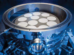
This MOCVD manufacturing system accommodates wafer sizes of up to 8 inches. Photos courtesy of Veeco.
Two leading manufacturers of MOCVD equipment are Aixtron AG of Aachen, Germany, and Veeco Instruments Inc. of Plainview, N.Y. James T. Jenson, vice president of marketing for the LED business unit at Veeco, said that the greatest concern for LED manufacturers is economics.
“We’ve looked at LED manufacturing costs from the substrate coming into the LED line in the factory through the epi step and chip processing, all the way through final packaging.” By increasing the yield and improving the process and tool architecture, he estimates that costs can be reduced fourfold from 2009 to 2013.
A few considerations that go into achieving the overall cost reduction include increasing automation, using a larger wafer size and improving the processes to ensure a higher throughput of very high quality LEDs. Although Semenza noted that one advantage of MOCVD is greater throughput and larger wafer size, the leading equipment manufacturers want to lower manufacturing costs while boosting output even further.
Jenson said that Veeco examines the cost of the epitaxial process on a square-centimeter basis, which requires looking at the labor that goes into using the epi tool. “The MOCVD process is a lot more labor-intensive than traditional semiconductor manufacturing. By lowering the epi cost while improving yield, you’ve improved everything. In other words, there is a multiplier to the cost benefit that occurs on the downstream processing when the epi step is improved.”
Manufacturers also are paying close attention to the growth rate because speeding up the rate will improve process time. There are various ways of doing this, including tailoring gas-flow dynamics, adjusting chemistry concentrations and optimizing the temperature environment. The catch is not to compromise the end result for the sake of faster output.
Automation also is helping to improve process time. By using loaders on the reactors, the number of wafers in a batch or the speed at which they are loaded can be increased. And by automating the loading process, common human error is eliminated. Veeco has a tool that automatically moves the wafers in and out of the reactor, a hands-free operation that eliminates the need to open the reactor by hand, release its vacuum pressure and lower the temperature. By maintaining the reactor under vacuum and at the proper temperature during wafer loading and unloading, productivity remains high.
LEDs for backlighting
LEDs come in a variety of flavors for a variety of applications. Those for general illumination are color-tuned to emit bright whites. Signal lights used in automotive applications are manufactured in specific colors and sizes. LEDs used for notebook computer backlighting are very small and use low to medium power. They usually are on the order of 0.3 x 0.3 mm on a side and can be mounted on the edges or behind a display. When lit, a diffuser plate and optics control the light so that it appears uniform behind the display.
For backlighting, LEDs offer additional advantages: Their small size allows for extremely thin displays, and they can be turned on and off as needed, enabling “local dimming.” For example, when an area on a TV screen is supposed to be dark, a screen lit with fluorescents would have to shut off a whole series of tubes, whereas an LED backlit display can simply turn off the LEDs behind that dark area. This improves the contrast ratio and is a benefit that is seeping into marketing campaigns for some of the leading TV ads.

With uniform chemical flow of critical importance, this system uses a patent-pending technology that ensures a consistent flow pattern of alkyl and hydride across all wafers.
One challenge, however, is in ensuring the consistency of film thickness. The whole process can take from six to 11 hours, a period during which many things can happen. Temperature control is critical, especially when it must be changed for a specific period. Being able to do it precisely affects the final outcome. Controlling the gas entering the chamber also is critical because each wafer must receive the same gas or chemical process to ensure consistency of the end product. Thus, both temperature and gas flow must remain constant throughout the process – and from run to run.
We are now seeing MOCVD systems with state-of-the-art reactor technology for high-volume production with process control. With LED manufacturing at an all-time high, demand for these systems is strong and growing. In addition, MOCVD process systems are used in space-based solar and concentrated photovoltaics – two areas that also are seeing unprecedented demand.
Semenza said that, with only a handful of manufacturers of MOCVD equipment, “the market is certainly ripe for new entrants.”