A fluorescence microscope being developed by imec researchers will be able to achieve high throughput and high resolution, without a lens component. The technology could significantly speed up next-generation DNA sequencing and cellular research, as well as enable studies on larger scales.
Part of the trouble that researchers face with ordinary fluorescence microscopes, said Niels Verellen, principal scientist at imec, stems from certain limitations of lenses. As magnification increases, throughput — or field of view — decreases.

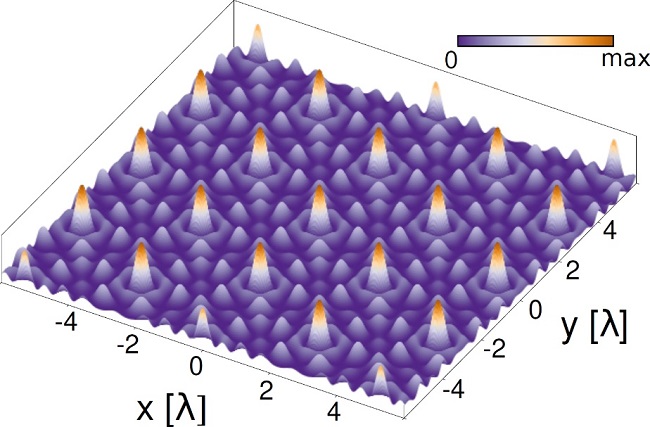
The light field's interference patterns can be precisely controlled to form illumination spots. Courtesy of Niels Verellen/imec.
“We are looking for a way to do fluorescence microscopy with high throughput, without compromising resolution,” Verellen told Photonics Media.
Traditionally, techniques for lens-free imaging use coherent light to perform a holographic reconstruction. With fluorescence microscopy, there is no coherence.
Verellen and his team used a scientific CMOS imager, similar to that found in a wide-field fluorescence microscope, as a foundation upon which to build its new device. The light source is coupled to the chip. “The main challenge of the whole concept lies in generating that light field in the chip we’re using for the excitation,” he said.

Niels Verellen, principal scientist at imec. Courtesy of imec.
The device’s main operating principle is the generation of a light field with multiple focal points, which enables the microscope’s high throughput.
“We want a grid over a large area to have a large throughput,” Verellen said. “The spacing between those light spots needs to be big enough to make this work.”
He and his team created a new mathematical model to generate the light field.
“It’s not at all a trivial situation,” he explained. “Very simply speaking, prime numbers come into play in this story, so prime number factorization gives us the solution on how to generate these patterns.”
The team set its sights on achieving focal points that were at least 200 nm, which is around where traditional fluorescence microscopes meet their limit. According to its calculations, 100 to 200 nm is within the realm of possibility. “We’ll aim for 100, but we may be closer to 200 nm,” Verellen said.
Explaining the technology’s structure and function, Verellen said, “What we have is a layer of material that can guide light, and on the surface of that material is a small part of the light that is leaking out. We use that light to excite fluorescence labels in the sample. Our magic is in structuring that light in the waveguiding layer in such a way that we make a grid of focal points, which allows the reconstruction of a high-resolution image. So we don’t need the lens, because in the end an integrated photonic circuit is taking the role of the lens in the microscope.”
Further, without the complex and bulky optics and objectives, the device becomes very small.
“One of the things I’m always thinking about is, you think about the biology lab and you’re studying some cell interactions, or your looking at cellular uptake of new medicine to see how it impacts those cells — you need statistics,” Verellen said. “So one measurement is not enough, so ideally you want to repeat this and have variations in your parameters. So if you have one microscope, it can take a long time to get there.
“Now, if for the same cost of that one microscope, you put 10 small chip scale devices on the same table, taking up the same amount of lab space, you’re improving your throughput immensely. And you can start thinking about setting up different kinds of experiments. Something that initially you were not able to investigate, because of time/throughput limitations, becomes possible, becomes feasible.”
Part of the research was published in Physical Review Letters (www.doi.org/10.1103/PhysRevLett.125.184101).