Dave Clark, Rajesh Patel, Jim Bovatsek and Wolfgang Juchmann, Spectra-Physics, a division of Newport Corp.
It is hard to ignore the many news stories about rising oil prices, higher energy costs, severe weather and concerns over global climate change. The emerging consensus is that we must reduce our reliance on fossil fuels and switch to cleaner forms of energy to avoid causing further damage to our planet. This view is being widely espoused across the political spectrum — even in the US — and has inspired renewed interest in alternative energy sources such as biofuels and wind, wave and solar power.
The invention of the “Bell Solar Battery” at Bell Labs in the middle of the last century was hailed as the future of electricity. But the high cost of solar cells has limited their deployment, and the promise has not been fulfilled yet.
Nearly 55 years after their invention, photovoltaic solar cells are generating only 0.04 percent of the world’s on-grid electricity. However, the situation is changing, and the solar industry looks set for explosive growth as it takes advantage of innovations enabled by lasers and manufacturing technologies derived from the flat panel display and the semiconductor industries (Figure 1).
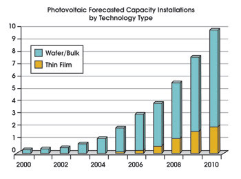
Figure 1. The historical and forecasted growth of photovoltaic capacity shows the relative share of thin films versus silicon wafers.
There are three basic types of solar cell technology: multijunction gallium arsenide, crystalline silicon, and various kinds of thin films on glass or metal substrates.
GaAs cells are fabricated using metallorganic chemical vapor deposition techniques on monocrystalline wafers and have the highest electrical conversion efficiencies (typically 28 to 29 percent but recently as high as 40 percent). These multijunction cells are expensive to manufacture and, therefore, usually limited to applications where cost is not an issue or where only small active areas are needed, such as satellites or solar concentrators.
Crystalline silicon cells are the most widely deployed and are made from either mono- or multicrystalline silicon wafers and have efficiencies typically in the 13 to 22 percent range.
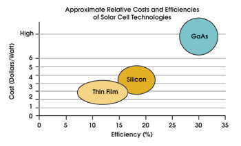
Figure 2. The ratio of cost versus efficiency for each technology is a constantly changing state.
Thin-film cells are a more recent entrant with slightly lower efficiencies (8 to 18 percent) but also lower production costs. Figure 2 shows the approximate relationship between cost and cell efficiency at present. Cost versus cell efficiency is a constantly changing picture as researchers and innovators strive to increase the efficiency and to lower production costs of each solar cell technology.
Crystalline silicon shortage
Crystalline silicon cells account for more than 93 percent of the photovoltaic market. In 2006, solar surpassed the semiconductor industry in its usage of silicon wafers, accounting for some 55 percent of consumption worldwide (Figure 3). The rapid ramp in demand for wafers has created a shortage in the feedstock supply and has temporarily pushed the price of silicon cells higher. This has motivated the industry to look more seriously at alternative thin-film technologies, which use little or no silicon.
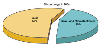
Figure 3. Solar applications now account for more than 55 percent of the silicon wafers consumed worldwide.
Thin-film solar cells generally consist of multiple layers of different materials coated onto a glass or metal substrate: A typical cell structure is shown in Figure 4. The most common absorber materials used are amorphous silicon, cadmium telluride and copper indium gallium diselenide. Usually, transparent conductive oxides such as indium tin oxide or zinc oxide and metals such as aluminum or molybdenum form the outer electrodes of the cell. Diode-pumped solid-state lasers are used to scribe interconnect and isolation patterns at various stages of the manufacture of the panel. Figure 5 shows a schematic cross section through a typical amorphous silicon cell with three laser scribes.

Figure 4. This schematic shows a cross section through a thin-film amorphous silicon (a:Si) solar cell. The P1, P2 and P3 scribe patterns create an array of individual series connected cells. TCO = transparent conductive oxide.
Laser scribing
The first step in creating thin-film solar cells is to coat the front electrode onto the glass substrate. The coating is usually indium tin oxide — a transparent conductive material. Then, the P1 electrode pattern is scribed, usually with a Q-switched solid-state neodymium-doped vanadate laser operating at the fundamental wavelength (1064 nm) and using around 12 to 15 W of average power.
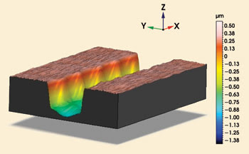
Figure 5. This P1 layer of indium tin oxide on glass was scribed with a laser.
For high throughput, it is necessary to scan the beam rapidly and to operate the laser at a high repetition rate of ~100 kHz or above. The laser should have a narrow pulse width of 15 to 40 ns to ensure that the peak power is above the material ablation threshold, even at these very high repetition rates.
Ideal lasers for this process step include the Spectra-Physics Navigator YHP40-106Q or Hippo H10-106Q. Hundreds of these lasers are installed in photovolatic scribing machines worldwide. Beam quality and pulse-to-pulse stability are also very important for a clean scribe and a reliable and repeatable process. For even faster throughput, some manufacturers are investigating other wavelengths and lasers that can operate at even higher repetition rates.
Once the indium tin oxide is patterned, the panel goes back into the chemical vapor deposition machine, where it is coated with the semiconductor — in this example, a thin layer of amorphous silicon. This is then patterned with P2 scribes using, in most instances, a green 532-nm neodymium-doped vanadate laser from the back through the glass.
Again, high repetition rates are a requirement for fast throughput, and short pulse widths of 15 to 30 ns are ideal. In this case, the power requirement is much lower, usually less than 1 W, so either a low-power green laser can be used or the beam from a 4- to 6-W laser can be split to perform multiple scribes at once.
When the P2 scribes are completed, the panel is coated with the back contact, which is usually aluminum, and then laser scribed with the final pattern, P3. This also is done from the back through the glass with a laser identical to the one used for the P2 process. Again, beam quality and pulse-to-pulse stability are very important for a good scribe and for avoiding damage to the underlying layers. Ideal lasers for the P2 and P3 process steps include the Navigator X15SC-532Q or Hippo H10-532Q.
Lowering costs
The main advantage of the thin-film panel technology over crystalline silicon is that it is scalable and lends itself to automated in-line processing. Companies that manufacture the in-line coating machines for the flat panel display market, such as Applied Materials, Oerlikon, Ulvac and Leybold, have recognized this opportunity and have started to develop turnkey production lines. The theory is exactly the same as in the display market — scaling up in the substrate area reduces costs because the equipment is used to manufacture scales at a different rate (Figure 6). Laser systems are a critical piece of these in-line production systems.
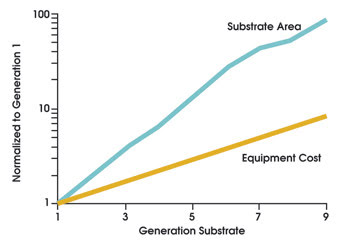
Figure 6. Costs of manufacturing equipment scale up at a different rate to substrate area; therefore, the cost per unit area reduces as the panel size increases.
Once more, the laser is playing a key role in bringing to reality a technology that has shown promise for decades. Just like in the semiconductor and display industries, lasers are helping to cut the cost of production and are brightening the future of the solar industry.
Meet the author
Dave Clark is director of strategic marketing, Rajesh Patel is applications lab manager, Jim Bovatsek is an applications engineer, and Wolfgang Juchmann is senior product manager, all at Spectra-Physics, a division of Newport Corp. in Mountain View, Calif.