Etching, scribing and isolating are essential functions in solar cell manufacturing, and lasers play a large part in each.
Solar cells turn light into electricity. So it’s fitting that electricity converted into light – a laser – plays a vital role in making solar cells. Through laser scribing, isolating and etching, many solar cells made today undergo light-driven material removal during manufacturing. Researchers are investigating ways to improve and extend these processes, further boosting the performance while cutting the cost of solar cells. However, market conditions may delay the implementation of such innovations.
For now, lasers help make solar cells more cost-competitive, according to Chris Eberspacher, president of Santa Clara, Calif.-based Hanwha Solar America. He’s also advanced technology officer of Hanwha’s worldwide solar business.

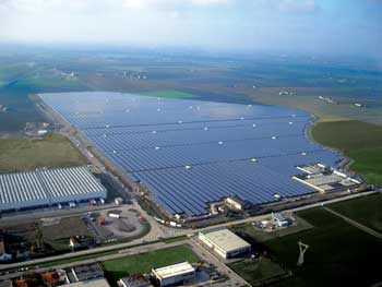
A 70-MW direct-current (DC) solar cell plant in Rovigo, Italy, generates enough energy to power more than 16,500 homes. Lasers are used for high-speed trench isolation in solar cell manufacturing.
“Today lasers are very widely used to do a shallow trenching in order to isolate, in effect, the front of the solar cells from the back,” he said.
To see why this is necessary, consider that the mass production of the dominant form of silicon-based solar cells begins with a crystalline 15-cm-or-larger p-type wafer, similar to what is used by the $300 billion semiconductor industry worldwide. This wafer is then coated with an n-type dopant, with diffusion creating the buried p-n junction necessary for the photovoltaic effect. However, it is not cost-effective to use a mask during the process. Therefore, the junction wraps around the edge, electrically connecting the front of the wafer to the back.
The solution employed by many high-volume manufacturers is to use a laser system. Taking only a second, these systems send a pulsed beam along the edge of the wafer, creating a trench that severs the connection from front to back. System parameters are juggled to optimize expense and throughput.

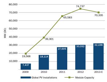
Worldwide, the growth in photovoltaic annual installations has slowed, leading to a large excess in module production capacity. If past trends had continued, installations would have reached 50 GW DC this year, instead of just over 30.
The latter is particularly important, due to the volumes involved, said Eberspacher. Significant strides have been made, with the time to do the isolation dropping from 90 seconds down to a single second.
On the verge of high-volume manufacturing is another laser-etching application. As solar high-efficiency local-contact cells are built, they must at some point be electrically connected to the outside world through low-resistance metallized contacts and traces. Doing so in the optimum way makes certain that the greatest number of photon-generated charge carriers are collected and
not lost.
Making those metallic connections involves removing protective insulating material. Here, femto- and picosecond pulse width lasers are being looked at to either vaporize the material or pop it off through photomechanical stress. The latter approach offers some advantages.
“It is a cold ablation process. There is not too much heat, and so it does little damage,” said Yafu Lin, a research engineer with Hanwha Solar America who specializes in laser processing of solar cells.
However, ablating insulating layers tens of nanometers thick does create debris. This is removed during the process with a particle fume extractor, Lin said.
Other potential laser applications involve forming finer metallic contact lines than is possible with other techniques. This could minimize shadowing of the active surface by metal traces. Yet another use of the beam could be as a localized energy source to significantly reduce contact resistance. However, in any laser-powered technique, total processing time has to be no more than roughly one second per wafer. Additionally, the laser systems have to run reliably in manufacturing lines producing millions of solar cells a day.
Crystalline silicon in the form of wafers may be the dominant photovoltaic material, but it’s not the only one. First Solar of Tempe, Ariz., uses thin films of cadmium telluride in a process that ultimately depends upon laser etching of various layers to create functioning product.

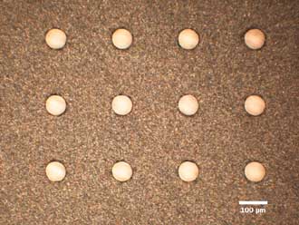
Back-side contacts in a crystalline silicon photovoltaic cell drilled by laser, allowing for a low resistance
connection and higher carrier collection efficiency.
“The semiconductor – the cadmium telluride – is applied to the glass via a vapor deposition process. We then use a laser to scribe cells,” said company spokesman Alan Bernheimer.
The advantages of this approach are processing times measured in hours instead of days, up to a 99 percent reduction in the amount of semiconductor material needed, and the ability to directly produce substrates that measure 60 x 120 cm. Respectable conversion efficiencies are possible, with First Solar demonstrating a performance in 2011 that topped 17 percent. Crystalline silicon offers higher numbers, with record efficiencies of 25 percent. However, in some configurations, First Solar’s technology can produce energy at a lower cost than silicon.
A downside is that unlike with silicon solar cells, no large established industry exists to piggyback on for progress in materials, tools or processes. Of course, this also means that there is less competition for raw materials. Additionally, care must be taken to ensure that the toxic metal cadmium is not released before, during or after module manufacturing.
Other thin-film contenders exploit different materials, such as silicon, copper indium selenide or cadmium sulfide. In general, all consist of a photon-absorbing thin film called the P2 layer; a back contact, the P1 layer; and a transparent conductive top coat, the P3 layer. Only the top micron or so of the silicon in a doped wafer actually produces electricity through the photovoltaic effect. The rest, which can be hundreds of microns thick, is merely supporting structure and added expense.

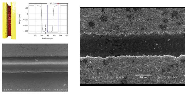
Using lasers, researchers scribed channels in a layer of (Left) molybdenum and (Right) copper indium selenide, similar to the back contact and photon-absorbing layers, respectively, found in thin-film solar cells.
Manufacturing of thin-film solar cells entails successive depositions of layers onto a substrate, which could be glass or even a flexible plastic. The resulting films then have to be scribed, or etched, to produce distinct cells. In the past, this has been done using mechanical means, a process that is slow and demands the exertion of a carefully controlled amount of force.
As is the case for other photovoltaic approaches, commercial success depends upon lowering the cost of manufacturing, and laser etching could help by speeding up the scribing process. Laser scribing can create fine lines that are tens of microns wide and a few deep. This can be done in a standard industrial setting, as opposed to the cleanroom needed for an alternative solution, lithographic patterning.
Optimizing laser scribing of the P1 and P2 layers is the subject of research by Yung C. Shin, a professor of mechanical engineering at Purdue University in West Lafayette, Ind. With mechanical techniques, scribing speed is typically less than 10 cm per second – leading to a long processing time, since total channel lengths can run into the kilometers.
The latest results from Shin and his group show scribing speeds of up to three meters per second, a thirtyfold increase, using a laser. What’s more, the channels so etched are straight and sharply edged, an important advantage.
“Etch quality of the microchannel is directly related to the efficiency of the solar cell,” Shin said.
In their work, the researchers used both a 1064- and 532-nm beam, with pulse widths of 10 ps. They optimized beam power and shape as well as pulse width. Before being used in volume manufacturing, the process will need to be commercialized, and there is no timetable at present for that. Similar laser etching techniques can be used to scribe channels on curved surfaces for flexible electronics, Shin said.
Laser manufacturer Coherent of Santa Clara, Calif., is one of the companies supplying lasers and systems to solar cell manufacturers. For edge isolation, the company offers a 355-nm, sub-ns pulse width laser that a scanner directs around a wafer’s edge. The resulting scribe lines are less than 30 µm in width and feature minimized subsurface damage, according to Coherent.
Spectra-Physics, a Santa Clara, Calif.-based division of Newport, is another supplier of lasers used in solar cell processing. Wavelengths vary from the ultraviolet through the visible and into the near-infrared. Pulse widths are a few tens of nanoseconds to femtoseconds, and the lasers are capable of firing up to 100,000 times a second.
“The market is very diverse. Each company has a different approach. So there’s not one unifying trend,” said Herman Chui, senior director of product marketing, in surveying the use of lasers in solar cell manufacturing.
Laser etching innovations and other improvements that lower overall cost should eventually be adopted. However, that might take some time as the solar industry is going through a downturn.
M.J. Shiao, a senior analyst with the solar-market tracking firm GTM Research, noted that 2013 should see growth of 7 to 10 percent in capacity installed annually. That sounds impressive, but over the previous five years, the industry averaged a 40 percent compound annual growth rate. The sudden recent slowing has resulted in an oversupply of manufacturing capacity.
The cost of solar panels stood at $2 an installed watt in early 2011 and fell to about 65 cents a watt by early 2013, Shiao said. Contributing factors for the drop include overcapacity, the scaling up of production lines, and manufacturing innovations. As a result, for the first time ever the rest of the system outside of the solar cell module itself accounts for most of the system total cost. However, there are still significant incentives to deploy laser-based and other technologies that cut the cost of the power-producing part of a photovoltaic system.
“The module still is the largest single line item for a PV system,” Shiao noted.