Technique overcomes some of the limitations of traditional dicing methods.
Maridel Lares, Hamamatsu Corp.
Wafer fabs continually face challenges in manufacturing semiconductor devices because the devices continue to get tinier and more complicated. Integrated circuits continue to increase in circuit density. Trends in chip design and materials, such as using die attach films and wafers as thin as 50 μm, add to the complexity of manufacturing.
In fabrication processes, wafer dicing plays an early and critical role in the quality of the final product. Two conventional methods for dicing wafers — blade dicing and laser ablation dicing — pulverize the wafer material in the cutting path (known as dicing street or kerf). In doing so, these techniques can cause problems such as debris, damage to the device and loss of precious semiconductor material.
A laser technique called stealth dicing can overcome these problems by cutting the wafer from the inside. The method involves two steps: subsurface laser-induced perforations of the wafer followed by tape expansion to separate individual chips.

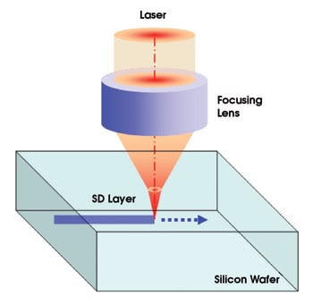
Figure 1. In stealth dicing, a laser beam that transmits through the wafer is focused beneath the surface, creating a row of perforations in a “stealth dicing” (SD) layer.
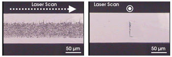
The initial subsurface treatment uses a pulsed laser beam at a wavelength that transmits through the wafer. For pure silicon wafers, near-infrared lasers are favored over short-wavelength lasers because of the absorption of shorter wavelengths by silicon. The pulsed laser beam is focused to a point beneath the wafer’s surface using an optical system (Figure 1). When the laser beam hits a peak power density at the focal point, the wafer absorbs the energy, and a pinpoint hole is created. The laser also causes compressive and tensile stress near the hole. As the laser beam travels the length of the wafer at a processing speed of 300 mm/s for a 120-μm-thick wafer, it perforates the inner layer of the wafer (Figure 2). The front and back surfaces remain pristine.

Figure 2. In the stealth dicing method, the laser beam creates perforations beneath the wafer’s surface. The front and back surfaces are not affected.
After laser processing, the wafer is still in one piece. The separation of individual chips occurs in the next step, when the tape upon which the wafer rests is expanded. The stress areas introduced by laser processing help this separation. A strong compressive stress around the hole is bounded on top and bottom by strong spots of tensile stress, and this sandwich of stress creates fissures along the laser’s path — like fault lines splitting the Earth — when the tape expands. Each chip is pulled free from the others. Thus, the cutting of the wafer originates from within the wafer and not from its surface.
The stealth dicing technique originally was developed by Hamamatsu Photonics KK in Japan for dicing ultrathin semiconductor wafers, but it has performed well on silicon wafers of all thicknesses and on specialty wafers with die attach films, low-k materials and microelectromechanical systems (MEMS).
The technique also may find use on other materials, including sapphire and glass. In addition, it is gentler to the environment than other methods because it is a dry process, reducing water consumption by 622 tons per year for each unit using the technology.
Dicing silicon wafers
Silicon wafers thicker than 100 μm traditionally are cut by diamond blades or saws, and the blade’s thickness, grit size, and rotating and cutting speeds affect the cutting quality. This technique has been refined over the years, yet it still causes problems that cannot be ignored. Chipping of the wafer occurs because of the force of the sawing process. The large cut width (kerf) caused by the blade wastes the wafer and produces debris that must be cleaned up. Other issues include wearing down of the blade over time and the cost of blade replacement.
For silicon wafers less than 100 μm thick, laser ablation offers an alternative to the blade technique, which is too powerful for the delicate thin wafers. However, laser ablation has its own problems. Vaporizing the wafer with a laser along the dicing path creates molten debris and microcracks. The debris deposited on the surface of the wafer is difficult to clean up, and the cracks result in chips with lower strength.
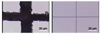
In contrast, stealth dicing does not generate the problems brought on by either the blade or laser ablation techniques. With stealth dicing, there is no chipping or debris, which eliminates the need for a cleanup process. It also reduces the amount of wasted wafer because of its very narrow dicing path (Figure 3), offering space on the wafer for more chips and higher production yield. Also, the technique does not cause heat damage because the laser cuts below the surface of the wafer; this contributes to rendering the chips more resistant to breakage.

Figure 3. Chips are diced from a 100-μm-thick silicon wafer by the blade method at a processing speed of 100 mm/s (left) and by the stealth dicing method at a processing speed of 300 mm/s (right).
Dicing specialty wafers
Specialty wafers — such as those with die attach films and those made of low-k material — and MEMS devices can pose problems for blade and laser ablation techniques.
Die attach films are used as adhesives for stacking and pasting multiple thin chips in a package. For the conventional blade method, the film adds another level of dicing problems because it is cut at the same time as the wafer; this can cause warping because the wafer and film have different mechanical properties.
However, stealth dicing handles these wafers with no problem. The wafer is laser-processed first, and then the die attach film is attached to the wafer. When the tape expands, the film is separated into the exact shape of the chips because of the very high adhesion forces between the film and wafer.
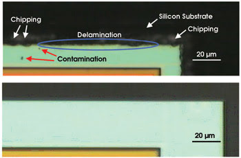
Low-k materials are widely used in chips to lower the dielectric constant of interlayer insulating films to allow higher-speed operation. For dicing wafers with low-k materials (especially ones that require a completely dry process), conventional dicing processes cause chipping, debris and delamination as well as large kerf widths. Stealth dicing, on the other hand, produces a clean cut (Figure 4).

Figure 4. Low-k device chips are shown being cut by the laser ablation method (top) and by the stealth dicing method (bottom).
MEMS are tiny mechanical electromechanical devices built on a silicon substrate and used in a variety of applications such as biotechnology and communications. These devices are very sensitive to external impacts, which makes stealth dicing an ideal method to use because it has a low external impact. No chipping or cracks occur, and extremely sharp edges are possible.
Stealth dicing offers a dry process, high speed, high quality (no chipping or debris) and low kerf loss. It is available as a laser module that is integrated with optical systems and that is incorporated into dicing machines. Currently, it is installed in Tokyo Seimitsu’s Mahoh dicing machine (ML200/ML300) and in Disco Corp.’s DFL7340/DFL7360 dicing machines.
Meet the author
Maridel Lares is a technical writer at Hamamatsu Corp. in Bridgewater, N.J.; e-mail: [email protected].