UPTON, N.Y., June 23, 2015 — A new laser patterning technique can create large-scale, nanostructured grids that could enhance manufacturing of optical coatings, solar cells and touch screens.
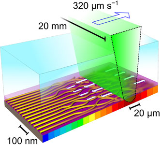
Developed at Brookhaven National Laboratory, laser zone annealing (LZA) involves sweeping a laser across a polymer sample to produce the extremely localized thermal spikes needed to drive ultrafast self-assembly of nanoscale cylinders. A heat-sensitive elastic coating on top of the unassembled polymer film expands when it is swept by the laser, which pulls and aligns the nanocylinders.

The sweeping laser generates intense heat that both accelerates polymer self-assembly and precisely aligns the nanocylinders that form the foundation of the final grid. Images courtesy of Brookhaven National Laboratory.
"Self-assembled structures tend to automatically follow molecular preferences, making custom architectures challenging," said Pawel Majewski, a postdoctoral researcher at Brookhaven. "Our laser technique forces the materials to assemble in a particular way. We can then build structures layer by layer, constructing lattices composed of squares, rhombuses, triangles and other shapes."
To make these 2D grids functional, the scientists converted the polymer base into other materials.
One method involved taking the nanocylinder layer and dipping it into a solution containing metal salts. These molecules then glom onto the self-assembled polymer, converting it into a metallic mesh. A wide range of reactive or conductive metals can be used, including platinum, gold and palladium.
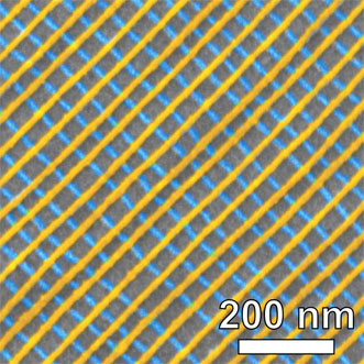
Vapor deposition can also be used to transform the nanocylinders into functional nanowires. The first completed nanowire array acts as the foundation of the full lattice. Additional layers, each one following variations on that same process, are then stacked to produce customized, crisscrossing configurations.

Scanning electron microscope image of a self-assembled platinum lattice, false-colored to show the two-layer structure.
"The direction of the laser sweeping across each unassembled layer determines the orientation of the nanowire rows," said Brookhaven scientist Kevin Yager. "We shift that laser direction on each layer, and the way the rows intersect and overlap shapes the grid. We then apply the functional materials after each layer forms. It's an exceptionally fast and simple way to produce such precise configurations."
Postdoctoral researcher Atikur Rahman said the process allows the stacking of metals on insulators, enabling different functional properties and interactions within one lattice structure.
"The size and the composition of the mesh make a huge difference," Rahman said. "For example, a single layer of platinum nanowires conducts electricity in only one direction, but a two-layer mesh conducts uniformly in all directions."
The research was published in Nature Communications (doi: 10.1038/ncomms8448).
For more information, visit www.bnl.gov.