Photonic lattices enable new applications for LEDs.
Alexei Erchak, Luminus Devices Inc.
LEDs have been around for close to half a century and have made steady progress, not the least of which is their availability in nearly every color. However, challenges remain, including the need in many applications for an array of LEDs that generates enough lumens.
LEDs traditionally are manufactured from compound semiconductors of materials grown using various epitaxy techniques, the most common of which is metallorganic chemical vapor deposition, which produces high-quality material that can convert electrical current into light very efficiently. However, most of the light never escapes the LED, because it is trapped by total internal reflection at the interface between the material with relatively high refractive index and the surrounding medium with relatively low refractive index.
 Partial solutions to this problem, including chip shaping, have improved the extraction efficiency but, despite these techniques, much of the light still remains inside the chip. Therefore, traditional LED chip sizes are kept relatively small (typically <1 mm2), so that the chip surfaces are closer to where the light is generated, reducing the losses related to total internal reflection that occur in larger chips.
As a result of the limitation in chip size, most high-brightness LED applications require an array of LEDs to generate sufficient lumens. LED arrays, however, pay a price of higher system complexity and cost along with reduced efficiency and reliability. In addition, brightness (defined as lumens/(solid angle × mm2)) cannot be increased by adding more LEDs, which limits LED array suitability for low-etendue applications such as rear-projection televisions.
Photonic lattice LEDs
Photonic crystals have received a great deal of attention over the past two decades because of their ability to control and manipulate the flow of light. By creating an intricate microstructure with feature sizes approximately equal to an optical wavelength, devices containing photonic crystals can have unique properties and can enable new applications in the areas of telecommunications, sensors, lasers and LEDs. In particular, photonic crystals create a new degree of freedom with much promise for constructing high-speed optical components. Despite massive investment during the telecom bubble, many of these applications never were realized. However, other applications of photonic crystals are starting to bear fruit.
A photonic crystal (sometimes called a photonic lattice) can be used to solve the light-extraction problem in LEDs by creating either a photonic bandgap (a range of frequencies in which light cannot propagate) or resonant optical modes that leak into the surrounding medium. This concept was proposed and patented first by a group at MIT in Cambridge. The nanoscale photonic lattice structures allow all of the light to escape from the surface of the LED chip independent of the device’s size. In addition, unique and beneficial properties, such as collimation, can be added using the photonic lattice.
Single large-chip illumination
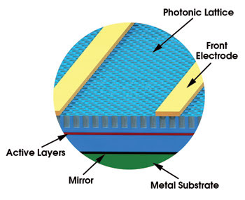
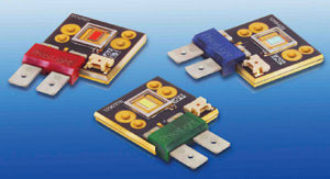
Luminus Devices Inc. of Billerica, Mass., built upon the photonic crystal LED by using the independence of light extraction from chip size due to the photonic lattices to create a scalable large-chip technology platform called PhlatLight (short for photonic lattice LEDs) that produces high brightness (Figure 1).

Figure 1. The PhlatLight chip has nanoscale photonic lattice structures.
Much of traditional LED chip design is not applicable to large chips. For example, traditional LED chips remain on the original growth substrate. For blue and green LEDs, the dominant growth substrate is sapphire, a poor thermal and electrical conductor. In the new design, the original growth substrate is replaced with a thermally enhanced substrate to enable vertical current flow and efficient heat extraction for the LED. A back reflector also is positioned between the substrate and the LED. It was important to pay close attention to the ohmic contact designs to spread sufficiently high levels of current across the entire chip. Failure to do so could have resulted in localized thermal runaway and a high rate of device mortality.
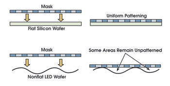
Packaging is critical for large-chip reliability and performance. Care must be taken to maximize thermal conductivity through all interfaces between the LED chip, the package, the board and the heat sink. Nanopatterning of the LED wafer with the photonic lattice also presents a particular challenge because wafers have nonuniform morphology as a result of defects created during metallorganic chemical vapor deposition (Figure 2). To complicate matters further for the nitride system, substantial curvature from the thermal mismatch between the sapphire substrate and the epilayers develops during the high-temperature metallorganic chemical vapor deposition growth.

Figure 2. Nanopatterning of LED wafers is complicated by their nonuniformity.
The design and process challenges for large-chip LEDs have been overcome. The LEDs are in full production and are finding their way into a variety of applications that demand high brightness and reliability under high-power operation (Figure 3). The first application to use this new technology was rear-projection televisions, in particular those based on digital light processing (DLP) from Texas Instruments Inc. of Dallas.

Figure 3. A single LED chip set is used to illuminate large-screen digital light procssing-based televisions.
The Achilles heel of rear-projection television always has been the high-intensity discharge lamps, which are prone to failure. LEDs have been sought after as an alternative light source, but the brightness from LED arrays was insufficient. This is the result primarily of etendue-conservation requirements dictating that the brightness of a source cannot be increased by attempting to combine multiple light sources illuminating a fixed area.
Today PhlatLight LEDs are used in all LED DLP televisions. A single chip set is used to illuminate the DLP chip with the RGB colors firing sequentially (Figure 3). Light collection and system efficiency also are greatly improved as a result of the collimation from the photonic lattice.
LCD TVs benefit also from this new technology. Today, cold-cathode fluorescent lamps are the dominant light source for backlighting LCD panels in LCD TVs. These traditional light sources have limitations in color gamut, in form factor and in power efficiency.

Figure 4. This Samsung 61-in. digital light processing-based high-definition television contains the Slim LED engine.
To illuminate a large-screen LCD TV with LED arrays requires thousands of LEDs, increasing system complexity and cost while dramatically reducing reliability, because one LED failure can take out an entire string of LEDs. In addition, LED brightness tends to change unpredictably over time, making this type of system too complex to control.
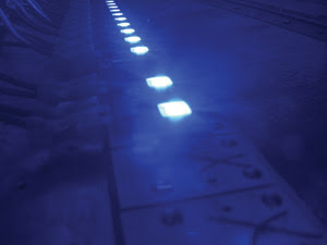
However, using this new large-chip technology, just a few LEDs positioned along the edge of a plastic waveguide can illuminate large-screen LCDs uniformly. Because just a handful of these LEDs are required, the color of each can be monitored and adjusted over time. LCD televisions that are edge-lit with these LEDs will be commercialized in 2008. Large-chip photonic lattice LEDs are being deployed also in other brightness-demanding applications such as entertainment, medical and architectural lighting.
Meet the author
Alexei Erchak is founder and chief technology officer of Luminus Devices Inc. of Billerica, Mass.; e-mail: [email protected].