AIM Photonics Leadership Seeks Industry Support, Explores Technology Goals
ALBANY, N.Y., Oct. 6, 2015 — Just two months after being selected to create a $610 million national manufacturing institute, a coalition of photonics researchers is aiming for a Jan. 2 launch date.
The American Institute for Manufacturing Integrated Photonics — AIM Photonics for short — already has an 11-member management team in place, and that group is moving rapidly to bring industrial partners into the fold and chart a course for the organization.
Integrated photonics devices, particularly those based on silicon, are expected to be crucial to communications and other technologies in the very near future. Until now, photonic integrated circuits (PICs) have been developed by several groups working separately, meaning there is no standard for assembly or packaging.
Creating that standard and finding ways to drive down manufacturing costs will be a primary goal of AIM Photonics. Today, as optical communications technologies reach for ever-higher data transmission rates, the advantages of a unified approach to fabrication and quality testing are clear, according to AIM Photonics CEO Michael Liehr.
"The timing for this thing is just right," he said in a recent phone interview with Photonics Media.
 Liehr, a former IBM researcher and executive, has been a professor at the State University of New York Polytechnic Institute's (SUNY Poly) Colleges of Nanoscale Science and Engineering for the last six years. He also was recently the general manager of the Global 450 Consortium, a group focused on developing the next stage of semiconductor fabrication technology using 450-mm wafers.
Turning his attention now to PICs, Liehr said an immediate priority for the next few months is convincing large companies to partner with AIM Photonics. A number of major companies including Intel Corp. and General Electric Co. have already pledged support. Liehr also highlighted telecommunications firm Infinera Corp. of Sunnyvale, Calif., which he said has already had commercial success with InP-based PICs.
AIM Photonics will be supported in its first five years by $110 million from the federal government, $250 million from New York state, and $250 million or more from other states and the private sector. Beyond that, Liehr said, AIM Photonics will need to rely on contributions from industry and generate its own revenue through licensing intellectual property.
"There's a very clear need for large companies to invest and to help us to become sustainable," Liehr said.
A membership drive will continue through the middle of next year, he said, with the goal of signing up 70 to 80 large, medium and small enterprises.
"Europe is ahead in industry coordination right now," following a decade of government investment, according to MIT professor Lionel Kimerling, another member of the AIM Photonics management team. Kimerling said the new institute will be "one of the first of this kind in the U.S., and the bet is that the innovation and research here, combined with the manufacturing capability, will allow our companies to really take off."
Setting goals
In the coming weeks, the AIM Photonics leadership council will choose a set of projects to invest in, and develop the institute's budget and goals. The organization has already sketched out four key technology manufacturing areas (KTMAs): data communications, analog radio-frequency (RF) devices, arrays and sensors.
Communications is currently the most mature application area, Liehr said, with several companies already working toward photonic integration for data centers and beyond. RF systems, meanwhile, will have a defense industry focus.
Arrays include lidar devices for remote detection and collision avoidance, as well as free-space communications, projection and displays, and bioimaging.
AIM Photonics Chief Technology Officer Michael Watts, a professor at MIT, has worked to develop single-chip lidar devices, which could eliminate the moving parts in existing devices and replace them with fixed, electrically steerable phased-array systems.

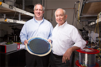
MIT professor Michael R. Watts, left, will serve as chief technology officer of AIM Photonics, while professor Lionel C. Kimerling will direct its education and workforce development initiative. Courtesy of Bryce Vickmark/MIT.
"Lidar systems that exist today are both bulky and expensive because they use mechanically scanned lasers," Watts said in a statement. But doing the same thing at the nanoscale, using phased-array systems on a chip, could drastically reduce size and cost, providing high-resolution, chip-scale, 3D imaging capabilities that do not exist today, he said.
Sensors are the least developed KTMA, Liehr said. While a multitude of photonic sensing technologies exist, they don't have many components in common, which will make it difficult to develop a multipurpose chip with wide appeal.
"We can't entertain something that is unique for each application," Liehr said. "Lots of people are working on it, but it's not clear what the main applications will end up being."
Research specialties
The work of AIM Photonics will be centered on universities in the coalition, which Liehr said bring different specialties to the table.
"They're all unique," he said. "We don't intend to replicate that but look at ways to coordinate them."
In New York, Columbia University will contribute high-speed testing capabilities. And Rochester — where the institute will be headquartered — has two universities and a large number of small- and medium-sized businesses that can offer packaging and system-level integration expertise.
SUNY Poly offers fabrication capabilities through its 300-mm semiconductor wafer line. The university has an existing collaboration with MIT that led to the first complete 300-mm silicon photonics platform, according to Watts. That effort has led to numerous subsequent advances in silicon photonics technology, with MIT developing photonic designs that SUNY Poly has then built.

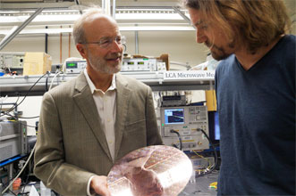
Professor John Bowers, left, and postdoctoral researcher Tin Komljenovic University of California, Santa Barbara, display a wafer integrated with photonic circuitry. Courtesy of Sonia Fernandez/UCSB.
Down the road, Liehr said, AIM Photonics will need to find a larger-capacity foundry. Being research-focused, SUNY Poly's fab has limited output, he said.
On the other side of the country, the University of Arizona will contribute optics expertise. Tom Koch, dean of the university's College of Optical Sciences, chairs the AIM Photonics Technology Advisory Board, which will oversee the portfolio of AIM Photonics projects. The Arizona Commerce Authority, meanwhile, has committed up to $2.5 million of tax incentives over the next five years to companies in the state that support AIM Photonics programs.
The West Coast division of AIM Photonics will be led by the University of California, Santa Barbara, which Liehr said is strong in laser research. Professor John Bowers, director of the university's Institute for Energy Efficiency, is deputy CEO of AIM Photonics.
University of California campuses in Berkeley, Davis and San Diego, as well as the California Institute of Technology, Stanford University and the University of Virginia, will also contribute research to the consortium.
Workforce development
MIT will also host the AIM Photonics program in education and workforce development, which Kimerling will direct. The program will develop educational materials to prepare future employees for this emerging industry, including teaching on the design of integrated photonic devices.
The AIM Photonics Community College Network will also facilitate workforce training. It will be led by Dr. Dale Allen, vice president for community engagement at Quinsigamond Community College in Worcester, Mass.
The network will support the creation of industry-recognized training modules for accelerated, stackable certificates based on local industry demands and create pathways to two-, four- and six-year degrees, the college said. The program could produce 50 to 100 students per year to meet workforce needs in central Massachusetts, where a number of photonics companies are located, Allen said in a statement.
Jacob Longacre, a photonics professor who is coordinating the curriculum development at Quinsigamond, said the college wants to work more closely with industry to react more quickly to technology trends.
"We are working with businesses to determine what type of training is needed, then we can develop curricula and offer streamlined packages of courses to meet those needs," Longacre said in a statement.