JPSA Expands Microprocessing Capabilities
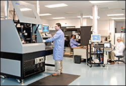
JP Sercel Associates Inc. (JPSA), a Manchester, N.H., provider of laser services and industrial ultraviolet laser technology, has expanded its microprocessing capabilities with new Class 10000 cleanroom  facilities and an IX-200 galvanometer-equipped laser material processing workstation. It said its job shop also offers expanded optics testing capability in an adjoining solid-state laboratory. Rick Slagle, sales and marketing director, said, “Our new cleanroom is essential for demanding medical and biomedical manufacturing applications . . . particularly with 193 and 248-nm wavelength processing.” The IX-200 “galvo” step-and-scan workstation can operate at 266, 532 and 1064-nm wavelengths and is suitable for applications including glass marking, high-speed hole or via drilling, and high-speed precision cutting, among other applications. JPSA shop performs wafer singulation and LED lift-off for the semiconductor packaging industry and micromachining of materials for biomedical research and medical product manufacturing.
/Buyers_Guide/IPG_Photonics_Microsystems_Div/c7267