By decreasing SWaP-C, CMOS image sensors will shape the future of embedded vision.
MARIE-CHARLOTTE LECLERC, TELEDYNE E2V LTD.
New imaging applications are booming: from collaborative robots in Industry 4.0 to drones that fight fires and monitor crops, from biometric face recognition to point-of-care hand-held medical devices at home. A key enabler in the emergence of these new applications is embedded vision, which has become more accessible than ever. Embedded vision is not a new concept; it simply defines systems that include a vision setup that controls and processes data without an external computer. Embedded vision is already widely used in industrial quality control, especially in smart cameras.

Recent changes have fueled the growth of embedded vision systems. One change to the industrial vision sector is the availability of affordable hardware components originally developed for consumer markets. This availability has drastically reduced the bill of materials and the size of embedded vision systems when compared to computer-based systems. Small systems integrators and OEMs can find
single-board computers or systems on a module (SOMs), such as the NVIDIA Jetson, in low volume; whereas larger OEMS can directly supply image signal processors, such as the Qualcomm Snapdragon or the Intel Movidius Myriad 2. At the software level, off-the-shelf software libraries have made specific vision systems much faster to develop and easier to deploy, even in fairly low quantities. Another change is the emergence of machine learning, which enables neural networks in the lab to be trained and then uploaded directly into the processor, so that the processor can autonomously identify features and make decisions in real time. The ability to provide solutions adapted to embedded vision is critically important for companies in the imaging industry that wish to target these high-growth applications.
Image sensors — which directly affect the performance and design of embedded vision systems — play a major role in increased adoption, and their key drivers can be summarized by decreased SWaP-C (size, weight, power, and cost). For embedded vision systems to be adapted to new uses, designers must be aware of market-acceptable price points that influence the cost of the vision system.
Compact optics
One way to lower the cost of a vision system is via footprint reduction. Reduced footprint matters for two reasons: 1) As the image sensor pixel size decreases, the intrinsic silicon cost shrinks (more chips can fit on the wafer); and 2) The sensor itself has been designed to fit with smaller and lower-cost optics. By reducing pixel size from 4.8 to 2.8 µm, for example, a full-HD image sensor would have its size reduced from a 2/3-in. optical format down to a 1/3-in. optical format. Smaller image sensors are compatible with more compact optics, which are far less expensive.
Indeed, the reduction of pixel size progressively enables image sensors of greater resolution to fit with smaller and more affordable optics. Whereas high-
resolution sensors (>5 MP) were previously only fitting with C-mount or F-mount optics, the market now sees more and more high-resolution sensors emerging that are able to fit with affordable
S-mount optics. This progressive shrinkage of optical format at equivalent resolution leads to great cost savings for vision module manufacturers because entry-level M12 lenses are generally priced 10 to 20× lower than C-mount or F-mount optics.
For image sensor manufacturers, this reduced optical cost has another impact on the design because, as a rule, the lower the cost of the optics, the less optimal the angle of incidence on the sensor. Less-expensive optics require the design of specific shifted microlenses positioned on top of the pixels so that they compensate for distortion and can focus light coming from wide angles.
Sensor interfaces
Optical optimization as well as choice of sensor interface indirectly affect vision system costs. The MIPI (mobile industry processor interface) CSI-2, which was originally developed for the mobile industry by the MIPI Alliance, is the most suitable candidate to enable interface-induced cost savings. Most image signal processors (ISPs) now use this interface, and it has begun to be adopted in industrial markets because it offers a lean integration in the cost-effective SOMs or systems on a chip (SOCs) from NXP, NVIDIA, Qualcomm, Intel, and others. Designing a CMOS image sensor with a MIPI CSI-2 interface provides a direct data transfer from the image sensor to the host SOC or SOM of the embedded system without any intermediate converter bridge. This design saves cost and printed circuit board (PCB) surface, and of course this advantage is even stronger in embedded systems such as those with 360° vision, which are based on using multiple sensors.
These benefits come with some constraints, however, as the MIPI interface has a connection distance limited to
20 cm, which may not be optimal in remote head setups where the sensor is located farther from the host processor. In these configurations, a camera board solution that integrates a longer interface is logical, but it comes at the expense of miniaturization. Some off-the-shelf solutions are ready to be integrated, including camera boards from industrial camera manufacturers FLIR, AVT, Basler, and others, and they are generally available in either MIPI or USB3 interfaces, the latter being able to reach 3 to 5 m.
Cost of development
When investing in a new product, development costs often present a challenge; they can require millions of dollars in nonrecurring expenses (NREs) and exert pressure on time to market. For embedded vision, this pressure becomes even stronger because modularity (defined by the ability to switch between image sensors) has high value for integrators. Fortunately, the NRE can be limited by offering certain degrees of cross-compatibility between sensors. This can be accomplished by 1) defining families of components that share the same pixel architecture to have steady electro-optical performances; 2) having common optical centers that share a single front mechanics; and 3) having a compatible PCB assembly that speeds up evaluation, integration, and the flow of the supply chain.
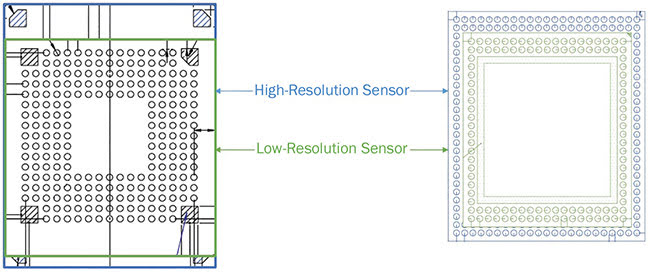
To ease the design of a modular camera board, or a board adaptable to several sensors, there are two ways to design a sensor package for scalability. Pin-to-pin compatibility is the preferred option for camera board designers because several sensors share the same electrical pads
and controls. This makes assembly transparent from a PCB design point of view. Alternately, by offering footprint-compatible sensors, PCB designers can use a single PCB for several sensors.
Designers, however, will have to anticipate multiple contact pads for each sensor and anticipate the PCB routing accordingly (Figure 1).

Figure 1. An image sensor platform can be designed to provide pin-to-pin compatibility (left) or footprint compatibility (right) between a high-resolution sensor (blue) and a low-resolution sensor (green), enabling a unique PCB layout design. Courtesy of Teledyne e2v.
Efficiency for enhanced autonomy
Miniaturized battery-powered devices, which include hand-held medical devices and glucose-monitoring smartwatches, benefit greatly from embedded vision technologies. Without the need for external computers and processing, portable devices can be designed to perform the same work as bulky systems. To decrease the energy consumption of these portable systems, image sensors include a multitude of features that enable the system designers to reduce power demand.
From the sensor standpoint, there are multiple ways to decrease power consumption in an embedded vision system without decreasing the acquisition frame rate. The simplest way, at the system level, is to minimize the dynamic operation of the sensor by using its standby and idle modes. These modes reduce the power consumption of the sensor itself. The standby mode, which works by switching off the analog circuit of the sensor, reduces the sensor’s power consumption to a couple of percent of the functional mode. Idle mode saves around half of the power consumption and can prepare the sensor to acquire images in microseconds.
Another way to save power is to design a sensor using more advanced lithography nodes. The smaller the technology node, the lower the voltage necessary to switch the transistors — which lowers the dynamic power consumption because it is proportional to voltage square, as shown:
Pdynamic α C × V2.
Therefore, switching from the 180-nm technology used 10 years ago to a 110-nm technology enables not only pixel-size shrinkage but also voltage reduction; the digital circuit voltages drop from 1.8 to 1.2 V. In the next generation of sensors, the 65-nm technology node will be used to provide even more power savings for embedded vision applications.
For additional power savings, appropriate image sensors can be chosen to reduce LED energy consumption in certain situations. Some embedded systems rely on
active illumination to generate, for example, a 3D map, or to freeze motion, or to simply increase contrast by using sequentially pulsing specific wavelengths. In these cases, the image sensor can generate power savings by lowering the noise of the sensor when operating in light-starved situations. By lowering the sensor noise, engineers can decide to reduce either the intensity of the current or the number of LEDs integrated in the embedded vision system. In other conditions, where image capture and LED flash are triggered by an external event, choosing the appropriate sensor readout architecture can lead to significant power savings. Whereas conventional rolling shutter sensors require LEDs to be turned on during the whole exposure of the frame, global shutter sensors allow it to turn on the light for only a portion of the frames. Switching from rolling to global shutter image sensors therefore saves lighting costs and also keeps the noise as low as the CCD sensors used in microscopy, if in-pixel correlated double sampling (CDS) is used.
On-chip functionalities
An extreme extension of this embedded vision concept is the full customization of the image sensor, integrating all the processing functions (by using SOC) in a
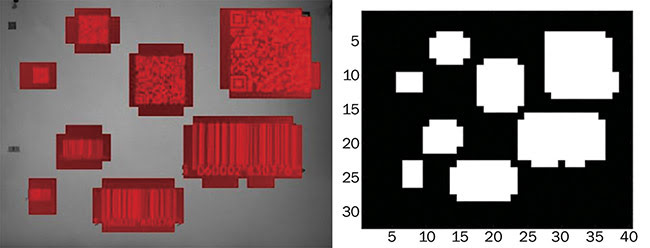
3D-stacked fashion to optimize performance and power consumption. However, the cost of developing such a product would be tremendously high. Although a fully custom sensor is not out of the realm of possibility to reach in the long term, today we are at an intermediary step, which requires embedding particular functions directly into the sensor to reduce computational load and speed up processing time. For instance, in barcode-reading applications, patented embedded features added onto the sensor chip now include a dedicated barcode identification algorithm that locates the position of barcodes in each frame, enabling the ISP to focus only on those regions, which helps the system process data more efficiently (Figure 2).

Figure 2. An automatic barcode location in an image sensor. A 5-MP image data output by the image sensor (left). A 1-byte image footer output by the image sensor (right). Courtesy of Teledyne e2v.
Another example of functionality that reduces the processing load and optimizes “good” data is a mode that enables the sensor to autonomously correct exposure time to avoid saturation when lighting conditions change. A feature such as this optimizes processing time because it can adapt to fluctuations of illumination in a single frame. This quick reaction will minimize the number of “bad” images that the processor needs to process.
These functionalities are often specific, and they require a good understanding of a customer’s application. As long as the application is sufficiently understood, additional on-chip functionalities can be designed to optimize the embedded vision system.
The smallest spaces
Embedded vision systems must be lightweight and fit into the smallest of spaces, such as within hand-held devices. For this reason, most embedded systems today use small optical format sensors (smaller than 1/2 in.) — with a limited
1 to 5 MP resolution.
One way to reduce the footprint and weight of the image sensor is to reduce the dimensions of the pixel array. The 65-nm process, presently being released, enables a reduction of the global shutter
pixel pitch down to 2.5 µm without damaging electro-optical performances. Such manufacturing processes lead to products such as a full HD global shutter CMOS image sensor in the same format as that used in the mobile phone market (less than 1/3 in.).
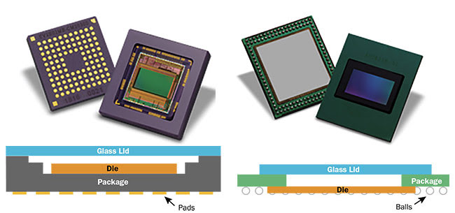
Another way to shrink sensor weight and footprint is to reduce the dimensions of the package. Wafer-level packages have experienced fast growth in the market over the last few years, especially for mobile, automotive, and medical applications. Compared to the classical ceramic land grid array (CLGA) packages used in the industrial market, the wafer-level
fan-out packages provide higher-density connections, which are an excellent solution to the challenge of producing miniature and lightweight image sensors for embedded systems. Wafer-level packages are also twice as thin as the ceramic packages and offer a 30% surface reduction (Figure 3).

Figure 3. The same die is assembled in a CLGA package (left) and in a wafer-level fan-out organic package (right) to reduce footprint, thickness, and cost. Courtesy of Teledyne e2v.
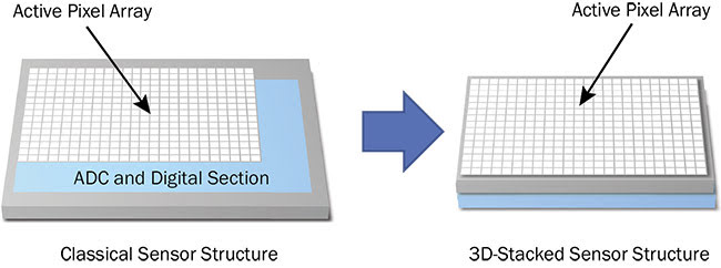
In the future, we can expect another technology to bring even further reductions in the size of sensors for embedded vision. This technology, 3D stacking, is an innovative technique for making semiconductor components by manufacturing the various circuit blocks on separate wafers and then stacking and interconnecting them with Cu-Cu (copper-to-copper) connections and through-silicon vias (TSVs). 3D stacking enables the manufacture of sensors with footprints smaller than conventional sensors. In 3D-stacked image sensors, the readout and processing blocks can be moved below the pixel array and row decoder. The footprint therefore decreases according to the surface of the readout and processing blocks, while also offering the possibility of adding extra processing power in the sensor to unload the image signal processor (Figure 4).

Figure 4. 3D chip-stacking technology enables an overlapped pixel array, as well as analog and digital circuits. It can even add extra layers of application-specific processing while reducing sensor footprint. ADC: analog-to-digital converter. Courtesy of Teledyne e2v.
To be widely adopted by the image sensor market, 3D stacking will have to overcome challenges. First, this is an emerging technology, and second, its costs will need to come down. It is more expensive because of the additional process steps required. These additional steps increase the silicon cost by more than 3× compared to conventional technology wafers. Therefore, 3D stacking will be an option mostly for high-performance or very small-footprint embedded vision systems.
Implementation of embedded vision can be summarized as practicing a “lean” vision — one that can be applied by a number of companies, including OEMs, systems integrators, and manufacturers of standard cameras. “Embedded” is a generic term that is used in many applications, so it is difficult to create a single list of specifications for it. But when it comes to optimizing embedded vision systems, markets are generally not driven by state-of-the-art speed or sensitivity, but rather by SWaP-C.
The image sensor can be a significant factor in SWaP-C parameters, so care is needed when choosing a sensor that will optimize the overall embedded vision system performance. The right image sensor will offer more freedom for an embedded vision designer to reduce not only the bill of materials but also the footprint of both illumination and optics. It will also offer a larger choice of affordable and deep-learning-optimized ISPs from the consumer market, without adding extra complexity.
Meet the author
Marie-Charlotte Leclerc is product marketing manager at Teledyne e2v Ltd. She has an engineering degree in semiconductors, an MBA, and a master’s degree in optics and semiconductors.