A uniform, or “top hat,” beam profile often is obtained at too great a cost. Laser remapping systems offer a high-throughput approach to beam shaping.
Kurt Kanzler, Lambda Research Optics Inc.
The Gaussian beam profile of a TEM00 laser is suitable for many applications. For targeting and alignment, the peaked Gaussian beam enables pinpoint precision. However, it is not ideal for other applications, including lithography, biomedical illumination and materials processing.
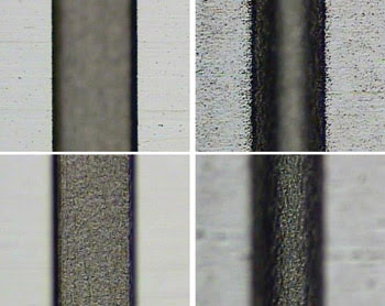
For example, Figure 1 compares channels micromachined into stainless steel with a Gaussian beam and with a beam whose intensity profile resembles a gentleman’s top hat — flat across the top with steep, smooth sides. Clearly, the top-hat beam produces superior results. The sides and bottom of the channel are smooth and flat, and the edges are better defined than those produced with the Gaussian beam.

Figure 1. The channel in the left-hand images was micromachined into stainless steel using a femtosecond laser with a relatively flat, uniform beam profile. The channel in the right-hand images was micromachined using a similar laser with a Gaussian beam profile. In the top photos, the focus is at the surface of the steel. In the bottom, it is at the bottom of the channels. Courtesy IMRA America Inc.
Techniques to smooth a Gaussian intensity profile are available, but they result in lost power. The choice of approach determines how many valuable photons are thrown away in the conversion of Gaussian beams into smooth-profile beams. Laser remapping systems offer particularly high throughputs.
Beam shaping
In general, there are three types of beam-shaping systems. The first is the simple aperture or mask. The second is the beam integrator, sometimes called a fly’s-eye lens. The third is the remapping beam shaper.
Most of us are familiar with the simple, round aperture. If an aperture is illuminated with a laser beam, the aperture geometrically defines the edges of the beam for a short distance. As a result of diffraction, the intensity changes quickly as the beam propagates beyond the aperture. Many laser users reimage the aperture to the working plane with a multielement optical system, and this approach to beam shaping is limited by the energy throughput at the aperture and the collection cone angle of the reimaging system.
In a beam integrator, multiple-aperture optical elements, such as in a microlens array, break the input beam into many beamlets and recombine them at a fixed plane. This method is useful for laser beams that have a high M2 value, such as excimer lasers. Beam integrators may be used with a mask reimaging system to create highly uniform excimer beams for applications such as laser annealing. Typically, the approach converts on the order of 40 percent of the incident power into the desired beam profile.
A laser remapping system uses a diffractive grating or a refractive lens to redistribute the input energy and map it to the output plane. This process can preserve the phase properties of the input laser beam. Remapping optics work well in applications that require the simultaneous control of phase and intensity.
Diffractive laser remapping also offers high energy throughput. With short-wavelength ultraviolet (e.g., 355 nm) systems, the approach converts more than 80 percent of the energy in the incoming beam to a top-hat profile. In the infrared (e.g., 10.6 μm), the performance can be even better, with more than 95 percent of the energy converted to the top hat. Diffractive remapping can shape a beam with a steep sidewall slope comparable to an aperture-based reimaging system, and it offers design flexibility, creating square, rectangular or high-aspect line shapes with a single optical surface.
Improved throughput
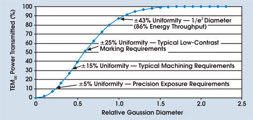
The peak-to-valley (PTV) uniformity of a beam can be defined as the difference between the maximum and minimum intensities, divided by the maximum intensity. This parameter provides a useful quantization of beam uniformity. The PTV of the portion of a Gaussian beam contained within a circle defined by the 1/e2 intensity is (1 – e–2)/1 = 0.86 = ±43 percent.
Because 86 percent of the energy is contained within this circle, we see that — at least for the part of a Gaussian that is fairly linear — the PTV is roughly equal to the energy encircled. For example, if a PTV of ±5 percent is required — for lithography, biomedical illumination or semiconductor annealing — an aperture would encircle only about 10 percent of the energy in a Gaussian beam. The other 90 percent would be wasted.
A quantitative perspective on the amount of energy thrown away with an aperture-based system is presented in Figure 2. From it, we see that the estimate that approximately 90 percent of the energy is wasted is correct. In this case, a diffractive beam shaper offers a throughput improvement of as much as a factor of nine.

Figure 2. The graph shows the percentage of energy (power) in a Gaussian beam transmitted through a given aperture. The horizontal axis is the aperture diameter, normalized to the 1/e2 intensity diameter of the Gaussian beam. The arrows indicate the beam uniformity required for various applications.
For applications such as microvia drilling, thin-film removal, precision high-contrast marking, microwelding, silicon-wafer dicing, precision glass machining, LCD panel repair and hard-disk texturing, a PTV of ±15 percent is acceptable. In this case, some 70 percent of the laser energy is wasted by an aperture system. Diffractive beam shaping would result in a throughput improvement of a factor of two or more.
Meet the author
Kurt Kanzler is manager of engineering projects at Lambda Research Optics Inc. in Costa Mesa, Calif.; e-mail: [email protected].