Laurent Fulbert, CEA-LETI
Being able to manufacture optical components within the CMOS processing infrastructure is key to realizing the potential of silicon photonics.
Photonics is a rapidly growing sector in the global economy. Optical communications, optical storage, imaging, lighting, optical sensors and security are just some of the applications for the technology. But although photonics could offer electronic components new capabilities such as low propagation losses, high bandwidth, wavelength multiplexing and immunity to electromagnetic noise, the high cost of photonic components and their assembly can be major obstacles to their deployment in many application fields. As with microelectronics, many applications can be realized in a much more compact and cost-effective way by integrating the required functionality in a single chip.
Silicon photonics (also known as CMOS photonics) is a way to tackle the cost problem by developing a small number of generic integration technologies with a level of functionality that can address a broad range of applications. Such technologies, which could be made accessible via foundries, could address markets large enough to pay back the development costs.
The Helios (pHotonics ELectronics functional Integration on CMOS) project proposes to integrate photonic components with circuits to enable a design and fabrication chain that can be transferred to European Union (EU) manufacturers. The project, a joint effort of leaders of the European CMOS photonics community, was launched in May 2008 by the European Commission (EC) within the Information and Communication Technologies theme of FP7, the Seventh Framework Programme. The 19 European partners aim to combine a photonic layer with a CMOS circuit by different innovative means. Coordinated by CEA-Leti, this four-year project has been awarded a grant valued at €8.5 million.
The project’s technological objectives include:
• Developing generic building blocks that can be used for a broad range of applications.
• Building and optimizing the whole “food chain” to fabricate complex functional devices, from design to the process level.
• Demonstrating the power of this proposed food chain by realizing several complex photonic integrated circuits addressing different industrial needs, including a 40-Gb/s modulator, a 16 x 10-Gb/s transceiver, a photonic QAM-10-Gb/s wireless transmission system, and a mixed analog-and-digital transceiver module for multifunction antennas.
• Investigating more promising but challenging alternative approaches that offer clear advantages in terms of integration on CMOS for the next generation of CMOS-photonics-based devices.
Key achievements
During the first three years, the project focused mostly on developing the key building blocks of silicon photonics. Starting from the isolated components, a strong effort has been made to increase the performance of each to allow system integration of state-of-the-art devices.
Light can be propagated in a silicon circuit using either rib (partial etching of the silicon film) or strip (full etching of the silicon film down to the buried oxide film) waveguides. The latter allows the highest compactness of the optical mode, but propagation losses are higher than those obtained with rib structures. A transition between rib/strip waveguides has been designed and fabricated with less than 0.2-dB measured losses. As for fiber coupling structures, Leti research has demonstrated an inverted taper coupling structure with 1-dB coupling loss, and Imec has demonstrated a high-efficiency grating coupler showing a coupling efficiency of —1.6 dB and a 3-dB bandwidth of 80 nm.
The integrated photodetector is one of the main building blocks for silicon photonics applications for either monitoring or high-speed detection. Germanium photodiodes exhibiting high responsivity (0.8 to 1 A/W), low dark current and high-bandwidth photodiodes (up to 130 GHz) have been designed, fabricated and characterized.
Silicon-based optical modulators use the plasma-dispersion effect that relates changes in the free-carrier concentration to changes in the silicon’s refractive index and absorption. Carrier depletion and accumulation, unlike carrier injection, are not limited by the relatively long carrier lifetime in silicon; consequently, the fastest reported devices have used these mechanisms. The modulator comprises a phase shifter (or phase modulator) inserted in a Mach-Zehnder interferometer. Different designs have been evaluated, such as thick modulators (i.e., using a 400-nm-thick silicon-on-insulator (SOI) substrate) or thin modulators (i.e., using a 220-nm-thick SOI substrate).
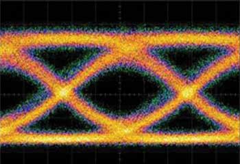
Figure 1. Silicon-based optical modulators use plasma dispersion, relating changes in free-carrier concentration to changes in the silicon’s refractive index and absorption. Silicon-based devices with lengths of 3.5 and 1 mm operating at 40 Gb/s have been demonstrated with respective extinction ratios of up to 10 and 3.5 dB. Here, an eye diagram of a 40-Gb/s silicon modulator. Images courtesy of Helios.
Recently, 3.5- and 1-mm-long silicon-based devices operating at 40 Gb/s have been demonstrated with extinction ratios of up to 10 dB and 3.5 dB, respectively (Figure 1). The efficiency and optical loss of the phase shifter is 2.7 V/cm and 4 dB/mm (or 4.5 dB/mm, including waveguide loss), respectively. Furthermore, the potential for slow light propagation as a means to enhance the modulation efficiency was demonstrated by means of a nanostructured 1-D periodic waveguide. Error-free modulation up to 20 Gb/s was achieved in a 500-µm-long silicon electro-optical modulator device.
Integrating lasers with silicon photonic-electronic circuits is a major challenge. The complexity lies in the fact that silicon is a poor light-emitting material due to its indirect energy bandgap. Helios has tried to overcome these silicon limitations by using the coupled system of erbium and silicon nanocrystals, and these efforts have resulted in the design of LED and laser structures. First, LEDs having 0.5 percent of external quantum efficiency and emitting at the wavelength of 1.54 µm have already been demonstrated, almost all the erbium in the structure has been inverted, and strong excited-state emission under electrical injection has been observed (Figure 2). Laser cavities using the same material are now being tested.
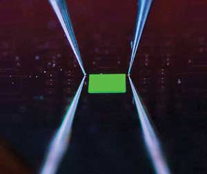
Figure 2. Silicon is a poor light-emitting material, thanks to its indirect energy bandgap, but Helios has tried to overcome this by coupling erbium and silicon nanocrystals. Here, green emission from an integrated erbium-doped LED.
The direct growth of standard III-V materials on silicon substrates is still a major obstacle because of the mismatch in lattice constants and in thermal expansion coefficients. A different approach consists of combining III-V heterostructures to silicon waveguides. It is based on die-to-wafer bonding of III-V material on top of a patterned SOI substrate. Then, hybrid silicon/III-V lasers are realized following a collective fabrication procedure, enabling complex photonic integrated systems onto the silicon platform. A first generation of Fabry-Perot-type devices exhibited continuous-wave operation at room temperature at 1.55 µm. The laser threshold is lower than 30 mA, with more than 2-mW output power coupled to a single-mode silicon waveguide. More advanced designs have been achieved, such as distributed feedback-type, distributed Bragg reflector-type, multichannel and ring resonator-based tunable lasers; these will be presented this year at IPRM (International Conference on Indium Phosphide and Related Materials) and GFP (IEEE Conference on Group IV Photonics) 2012.
Finally, innovative designs of III-V/silicon lasers have been developed using photonic crystal membrane reflector architecture for enhanced light control and optical-mode confinement.
Building the whole value chain
The satisfactory use of photonic design tools in an electronic design automation (EDA) flow is necessary for the deployment of silicon photonics. Helios is focused on developing a coherent design methodology and flow for the integration of photonics on CMOS covering all design and tool aspects from virtual fab to the system level. The project also will facilitate the electronic/photonic convergence at the design level by developing an interface strategy for the integration of photonic design tools with EDA tools. The environment currently in development will allow a continuum from architectural to physical design, photonics and electronics co-design, as well as the integration into EDA flow.
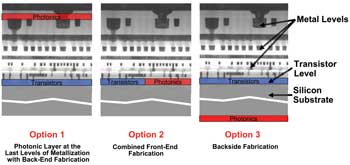
Figure 3. Photonics functionality can be added to an electronic circuit using one of three methods. Here, a cross section of a photonic-electronic integrated circuit showing the different integration options.
The photonics functionality can be introduced on an electronic circuit in three main ways (Figure 3). The first way Helios is exploring is the integration at the last levels of the metallization of the integrated circuit. The main advantages of this method are the physical independence of the electronics and the photonics layer, which avoids any change in the electronic library design and the possibility of using any technology (CMOS or SiGe). Figure 4 shows an example of the integration of a photonic on top of a CMOS circuit with wafer bonding using option 1.
The second way combines the photonics fabrication with the transistor fabrication at the front-end level. The thermal budget rules the process steps. The main issue is the lack of possible integration of the laser, leading to a classical flip-chip approach with some consequences on packaging.
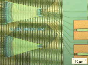
Figure 4. The integration of arrayed waveguide grating (AWG) and photodiodes on top of a CMOS wafer; this method corresponds to the first option depicted in Figure 3.
A third way that Helios is exploring is taking advantage of the rear side of the electronics wafer. Through-silicon vias connect the front processed side with the backside, which will be used for the photonics layer.
Toward more complex circuits
Several demonstrators addressing industrial needs are under fabrication:
• An integrated modulator with its electronic driver working at 10 Gb/s.
• Wavelength division multiplexing transmitters and receivers for access networks and multifunction antennas.
• QAM-10-Gb/s wireless transmission systems.
Figure 5 shows the response of a 16-channel arrayed-waveguide grating (AWG) 200-GHz receiver. It consists of a 2-D surface grating coupler, two AWGs with 16 channels, and 16 germanium photodiodes. First tests on bandwidth exhibited 20-GHz operation.
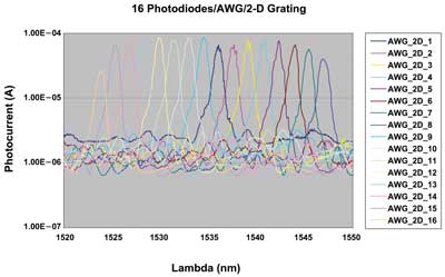
Figure 5. Response of 16-channel wavelength division multiplexing AWG 200-GHz receiver under random polarization. Initial tests on bandwidth exhibited 20-GHz operation.
A photonic QAM-10-Gb/s wireless transmission system consisting of a QAM modulator and a QAM demodulator have been designed and fabricated. Figure 6 shows a demodulator circuit that contains an inverted taper, a polarization diversity circuit, a tunable MZI switch, a delay line, 90° degree hybrid and photodetectors.
An integrated tunable transmitter incorporating a hybrid III-V/silicon laser fabricated by wafer bonding and a silicon Mach-Zehnder modulator exhibits 6-nm wavelength tunability, an extinction ratio between 6 and 10 dB, and excellent bit-error-rate performance at 10 Gb/s. This transmitter will be presented in September at ECOC (European Conference on Optical Communications).
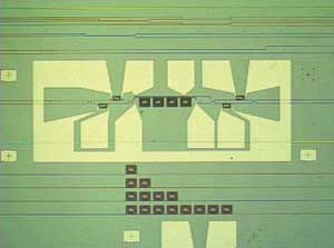
Figure 6. An optical image of the fabricated DQPSK demodulator circuit with an inverted taper, a polarization diversity circuit, a tunable MZI switch, a delay line, 90° hybrid and photodetectors.
Helios partners are focused on bringing CMOS photonics to foundries and component manufacturers for high-volume applications. After having constructed the toolbox for silicon photonics, the consortium is focusing on development of complex electronic photonic integrated circuits. This innovative technology is now available for Helios participants as well as others who need CMOS photonics to improve their products.
Meet the author
Laurent Fulbert is photonics program manager at CEA-Leti; email: laurent.fulbert @cea.fr.
Project partners
In addition to CEA-Leti, the Helios partners are:
Imec, Belgium
CNRS, France
Alcatel Thales III-V lab, France
University of Surrey, UK
IMM, Italy
University of Paris-Sud, France
Technical University of Valencia, Spain
University of Trento, Italy
University of Barcelona, Spain
3S Photonics, France
IHP, Germany
Berlin University of Technology, Germany
Thales, France
DAS Photonics, Spain
Austriamicrosystems AG, Austria
Technical University of Vienna, Austria
Phoenix BV, Netherlands
Photline Technologies, France
For more information, visit: www.helios-project.eu.