Imagine if a new substance could replace silicon, a material that is used in almost every electronic device on the market today. SiOnyx Inc. plans to do just that with its new material, black silicon, which was discovered at Harvard University in Cambridge, Mass.
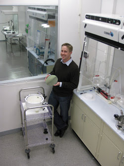
Dr. James E. Carey, SiOnyx Inc. co-founder and principal scientist, holds a black silicon wafer in the cleanroom at company headquarters in Beverly, Mass.
I recently sat down with Stephen D. Saylor, CEO of SiOnyx, and Dr. James E. Carey, its co-founder and principal scientist, at the company’s headquarters in Beverly, Mass., which is about 20 miles northeast of Boston.
Carey and Saylor told me that the potential applications of black silicon are numerous because it could be employed wherever silicon is currently used: in computers, satellites, cameras, mobile phone cameras, solar panels and radiological imaging equipment.
“We believe that the technology meets its highest purpose in the commercial markets,” Saylor said. The industry for silicon chips in mobile phone cameras alone is $7 billion, out of a $200 billion global market for silicon. “To get venture capital, you have to show that there is a big (market), and there is a big (market) in black silicon,” Saylor said. SiOnyx has raised $11 million in venture funding from RedShift Ventures, Polaris Venture Partners and Harris & Harris.
Black silicon is superior to conventional silicon because it is 100 times more sensitive to light. It also is sensitive to a broader spectrum of light – from the short-wave UV to the infrared. Therefore, black silicon could be used to make solar panels that capture more of the sun’s rays and cameras that are more sensitive to light.
On the other hand, detecting light may no longer be such a concern for engineers who design cameras once they get their hands on black silicon. “Very seldom do (camera engineers) have too much light, too much signal,” Saylor said. Imagine if camera engineers had a material that is 100 times more sensitive to begin with. It would free them of design constraints.
The broad spectral sensitivity of black silicon makes it attractive for infrared security cameras. Because ordinary silicon cannot absorb in the infrared at all, other materials, such as germanium or indium gallium arsenide, are used. However, these materials are expensive and toxic to humans, whereas black silicon is nontoxic and can be made inexpensively.
Black silicon may have a medical benefit as well because the radiation dose that a patient receives from CT scanners and other radiological equipment is directly proportional to the sensitivity of the detector. Black silicon does not detect x-rays, but radiological imagers contain a component called a scintillator that converts the x-rays into light that black silicon can detect.
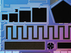
Black silicon photonic test structures. Such structures are commonly used in the development of new semiconductors to help design engineers and device physicists optimize performance and reliability.
Eureka moment
Black silicon was discovered by chance in Dr. Eric Mazur’s lab at Harvard. The researchers focused a femtosecond laser on silicon chips in the presence of sulfur hexafluoride gas, which is commonly used to etch circuits in semiconductors. Once the researchers turned off their equipment, they noticed that the surface of the silicon chip had turned black. They thought they had burned the surface, according to Carey, Mazur’s former graduate student.
A closer look at the black silicon with an electron microscope, however, revealed that the surface had rows and rows of spikes all over it. The rows appear neatly arranged on the surface, almost as if someone placed them there on purpose. It turns out that these spikes give black silicon its unique color and properties.
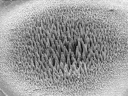
Black silicon has a remarkably well-ordered array of spikes on its surface, as shown in this electron micrograph.
Most researchers would have stopped once they had made the surface of silicon black, but the researchers in Mazur’s lab chose to investigate why it turned black. “That’s something credited to professor Mazur,” Saylor said, “If you had a lab where a professor was micromanaging (his students), this never would have happened.”
Mazur also is known for his work toward improving higher education by modifying or eliminating traditional lecture classes. He founded SiOnyx with Carey in 2006 and currently serves on its scientific advisory boards.
Forming a company
After obtaining the patent license from the university, the company hired Saylor. Saylor has an engineering degree and got his start in companies such as Apple, Polaroid and Technion. He started his own company, FlashPoint, and then worked for Adobe Systems before becoming CEO of SiOnyx. “I was an engineer who got frustrated that people on the business side didn’t understand the technology,” he said.
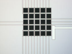
Black silicon test pixels, which are used to optimize imaging performance.
Of the company’s current employees, 95 percent are experienced engineers. If SiOnyx sounds like an exciting start-up to work for, Saylor said, “We’re always looking for good people.” He emphasized that, besides experience, potential hires must be able to fit within the company’s culture.
SiOnyx recently opened an office in Portland, Ore., because that city shares cultural similarities with Boston and because of the concentration of engineers with experience working with semiconductor materials.
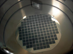
Processing a black silicon wafer in a chamber.
Saylor said the company wants to get black silicon into the hands of people who can work the raw material into circuits and sensors that can be placed into electronic devices. The company already has made a prototype of a common integrated circuit called a CMOS chip.
The price of the products that the company will offer will depend on the market. “A cell phone chip might cost less than a cup of coffee at Starbucks,” Saylor said, “but a chip in a satellite might cost …” “more than Starbucks,” Carey added, as if on cue.