Fraunhofer, EV Group to Enable Direct Semicon Wafer Bonding
FREIBURG, Germany, June 7, 2013 — Multijunction solar cells with conversion efficiencies approaching 50 percent could become cost-effective via a collaboration between the Fraunhofer Institute for Solar Energy Systems ISE and equipment supplier EV Group (EVG) of St. Florian, Austria.
The collaboration will work to develop electrically conductive and optically transparent direct wafer bonds at room temperature using mismatched material combinations such as gallium arsenide (GaAs) on silicon, GaAs on indium phosphide (InP), InP on germanium (Ge) and GaAs on gallium antimonide.
“Using direct semiconductor bond technology developed in cooperation with EVG, we expect that the best material choices for multijunction solar cell devices will become available and allow us to increase the conversion efficiency toward 50 percent,” said Dr. Frank Dimroth, head of the department III-V — Epitaxy and Solar Cells at Fraunhofer ISE. Such cells could lead to new device architectures with unparalleled performance.

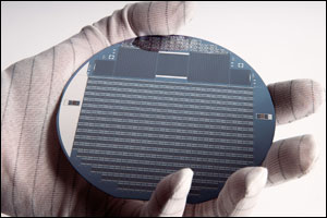
III-V multijunction concentrator solar cells on a 4-in.-diameter wafer. Courtesy of ©Fraunhofer ISE/PRNewsFoto.
Fraunhofer ISE has developed III-V multijunction solar cells with efficiencies of up to 41 percent with its metamorphic triple-junction solar cell technology on Ge, but achieving higher cell efficiencies would require the development of four- and five-junction solar cells with new material combinations that can span the full spectrum between 300 and 2000 nm.
“Fraunhofer ISE’s broad expertise in the area of PV [photovoltaics], specifically in concentrated PV cell manufacturing and photonics, will allow us to characterize bonding interfaces with respect to PV applications on our new ComBond equipment platform,” said Markus Wimplinger, corporate technology development and IP director for EVG.
EVG’s ComBond technology enables the formation of bond interfaces between heterogeneous materials — such as silicon to compound semiconductors, compound semiconductors to compound semiconductors, Ge to silicon and Ge to compound semiconductors — at room temperature, while achieving excellent bonding strength on substrates as large as 200 mm.
The technology also could be used in LED and silicon photonics applications.
For more information, visit: www.ise.fraunhofer.de or www.evgroup.com
/Buyers_Guide/EV_Group_EVG/c4622