Quantum forces create a sticky situation for microdevices
Since their advent in the 1980s, microelectromechanical systems (MEMS), micro-size machines with moving parts, have promised to revolutionize all aspects of industry by putting small, less power-hungry compact systems on a chip. But integrating MEMS into the mainstream has been slowed by poorly understood quantum forces that cause big trouble for small devices, compelling parts to slide or stick together in such a way that can prove fatal to the device.
MEMS, created using the same technology that makes integrated circuits, range in size from 1 to 100 μm, or about the width of a human hair. They are divided into two categories: sensors, which gather information about the world around them, and actuators, which perform specific tasks. They can contain optical components, such as mirrors, which makes them MOEMS (micro-optoelectromechanical systems).
Unlike integrated circuits that merely process electrical signals, MEMS devices are designed to perform functions such as pumping fluids, moving mechanically, measuring acceleration or dispensing medicine. Also unlike integrated circuits, MEMS are dependent on custom processing designed for each specific device. The first law of MEMS, “one product, one process,” refers to the fact that microdevice development is highly specialized, not standardized.

The MEMS accelerometer inside the Apple iPhone uses a silicon mass, a set of silicon springs, and an electrical current to allow it to adjust the display in response to motion. Image courtesy of Apple Inc.
Although hundreds of companies produce MEMS, the accelerometers and ambient light and proximity sensors used in the latest cell phones and other electronics are part of an exclusive group of MEMS that have made the leap from development to commercialization. Accelerometers, which can sense things such as tilt, motion, shock and vibration, are being used to detect when laptops are dropped, so the hard drive can be shut down and protected, or to provide Nintendo Wii players with the ability to have their physical actions mimicked by their on-screen character.
Other commercially successful MEMS include optical switches for telecommunications, gyroscopes for camera stabilization, inkjet printer heads, Dallas-based Texas Instruments Inc.’s digital micromirror device, pressure sensors used in vehicle airbags, and silicon microphones increasingly used in cell phones, hearing aids and other consumer electronics.

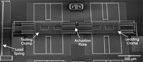
A scanning electron microscopy image of a double clamped beam adhesion force test structure. This microfabricated device is designed to measure adhesion forces in MEMS given a well-defined contact area. Courtesy of Ian Laboriante and Carlo Carraro, UC Berkeley.
So what is preventing MEMS from becoming more mainstream and replacing electronic components in a range of applications, particularly ones that can withstand harsh environments? Those working in the field say that, even after years of research, structural surfaces, surface coatings and other features that affect the performance of MEMS are not well understood. Because the surface-to-volume ratio in microdevices is much larger than it is for everyday objects, they are affected much more by surface forces such as stiction (said to be shorthand for static friction) and adhesion.

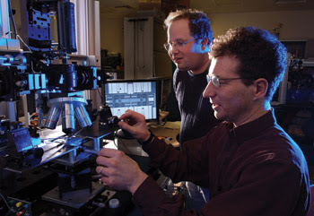
Maarten de Boer and Alex Corwin investigate friction at the microscale using a recently-developed nanotractor actuator fabricated using the Sandia Ultraplanar MicroMachine Technology (SUMMiT VTM) process. Courtesy of Sandia National Laboratory.
“We have done battle with [surface forces], and we’ve scored some victories, but it’s not like there will be a magic bullet that solves all these problems,” said Roger T. Howe, a professor in the department of electrical engineering at Stanford University in California who has researched MEMS since the early 1980s.
Also complicating efforts to design mainstream MEMS is the fact that, the smaller these systems get, the more quantum phenomena such as Casimir force and van der Waals (intermolecular forces) come into play, causing individual parts to attract, slide and/or stick together and often leading to catastrophic failure.
“It’s a much harder problem than what I envisioned when I first started working on it 14 years ago,” said Dr. Roya Maboudian, a professor of chemical engineering at the University of California, Berkeley. “But I think now we’re beginning to have a sense of the complexity of the problem. We’re refining the questions that we are asking.”
Anyone who has ever handled an Apple iPhone has experienced some of the most successful MEMS available on the market today. The cell phone uses a tiny accelerometer that detects movement and responds accordingly: Display a photo, rotate the phone, and it automatically changes the image from portrait to landscape view or vice versa by sensing how you’re holding it. It also has sophisticated sensors that dim or brighten the screen, depending upon ambient light conditions, and ones that turn off the display when you put the phone to your ear.
To create MEMS, microfabrication techniques are used to integrate mechanical elements and electronics onto a substrate such as silicon. The electronics are fabricated through processes used to make integrated circuits, while the micromechanical parts are made by selectively etching away parts of the silicon wafer or by adding new structural layers.
For simple applications such as a pressure sensor, MEMS can be made through bulk micromachining, a simple and fairly inexpensive process through which a silicon wafer is patterned. The pattern becomes a protective layer, with the unprotected parts of the silicon later dissolved away in a chemical solution.
More sophisticated applications may require that the MEMS be fabricated by surface micromachining, which builds the device layer by layer by depositing thin films on the silicon wafer. Patterning is done by selectively etching away parts of each layer of film. Moving, functioning machines are created by alternating the etched layers with spacer layers of a material that is later removed, leaving the structural elements free to perform.
“At the point of release, often you will see stiction if you’re not careful or the last step is not done properly. Even after a successful fabrication, if surfaces come into contact during the operation, adhesion is very often observed,” said Maboudian, who also is a faculty member at the Center on Interfacial Engineering for Microelectromechanical Systems (CIEMS), a collaborative research project at Stanford, at UC Berkeley and at Iowa State University in Ames.
The force is with you … unfortunately
Stiction refers to a number of quantum forces that draw tiny parts of MEMS and NEMS (nanoelectromechanical systems) together at the nanoscale.
“Stiction is a complicated collection of phenomena,” Howe said. “In the micro, or especially the nano world, things jump onto the gripper.”
“It is viewed that stiction is one of the key culprits limiting MEMS reliability,” Maboudian said. And even the cause of stiction itself isn’t that easy to pinpoint.
“Not all MEMS devices involve contacting surfaces; in such cases, the stiction that occurs is primarily during fabrication,” she said, so the device must be processed to avoid surfaces coming into contact during etching. “However, if the devices are contacting or prone to come into contact, surface forces must be carefully examined, even at the design stage.”
When and why stiction occurs can vary depending upon the design of the MEMS device, its fabrication process and the material from which it is created, so there is no easy, all-encompassing answer, she added.
“It’s hard to predict a priori if you design a MEMS device whether it’s going to adhere or not – there are quite a few variables affecting stiction, ranging from surface topography to the environments the devices are expected to operate in. In some foundries the silicon is very rough, and in some it’s not. Sometimes the materials composing different layers of the device are assumed to be the same, but slightly different processing makes one layer effectively different from another,” Maboudian explained. “Fabrication facilities can give specs on properties such as doping, stress and strain, but they don’t give specs on stiction.”
The design of the microdevice also plays an important role, she said. “For example, if you have two beams that are very long. The longer it is, the more compliant it is, and, hence, more prone to adhere upon contact.”
Maboudian also has been developing ways to modify surfaces chemically, reducing the surface energy by depositing Teflon-slick thin-film coatings, and also physically by roughening the surfaces.
Her group is exploring other materials for MEMS creation because silicon, the workhorse material of the microelectronics world, is more prone to stiction issues. “Partly because, chemically, it’s very reactive,” she said.

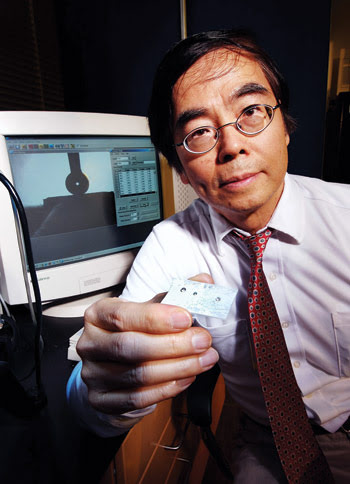
C.P. Wong, a professor in Georgia Tech’s School of Materials Science and Engineering, holds a sample of a self-cleaning coating developed in his lab based on the lotus plant. Courtesy of Georgia Tech.
“We’ve been looking at coatings to go on silicon or aluminum to act as lubricants or reduce net surface energy. Or even changing the material altogether, to silicon carbide or diamond. With silicon carbide, we are targeting harsh environments, situations where silicon would have a hard time: high temperatures, high pressure, high acceleration,” she added.
One key to being able to reduce or mitigate quantum forces is the ability to measure them accurately.
In 2004, researcher Maarten de Boer of Sandia National Laboratories’ Advanced Sensor Technology Department created a 500-µm-long actuator called the nanotractor as a tool to measure the friction on a MEMS device. He and colleague Alex Corwin discovered that adhesion forces cause deviations in Amontons’ law, a 300-year-old principle that friction force is proportional to normal (perpendicular) force. They found that the law is not valid over short sliding distances.
De Boer and his colleagues also found that, under dry conditions – i.e., no capillary forces – as surface roughness decreases, van der Waals forces between noncontacting portions of a micromachine’s surface increasingly contribute to adhesion. The researchers also have made other experimental and theoretical discoveries about the interplay between capillary forces, surface topography correlations, surface plasticity and disjoining pressure – the result of van der Waals repulsion.

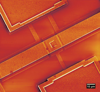
Scanning electron microsope image of the nanotractor. Courtesy of Sandia National Laboratory.
“We have recently developed a method to measure dynamic friction in a simple fashion. We have also found significant effects of measurement protocol, including frictional aging and deaging of monolayer coatings,” de Boer said. “These studies are very helpful in understanding how to manipulate friction in order to get a desired response.”
Controlling Casimir
Recognizing the importance of overcoming the Casimir force, DARPA’s Microsystems Technology Office announced in September an aggressive funding program, Casimir Effect Enhancement. The goal is to develop new ways to control and manipulate attractive and repulsive forces at the surface level, such as adhesion in nanodevices and drag on vehicles.
Besides manipulating and engineering the force, demonstrating the ability to totally neutralize the Casimir force is a specific goal of the program.
“The impact on the field could be spectacular if the targets are met. It could enable reliable operation of structures that are much more delicately suspended,” Stanford’s Howe said.
Success stories: Thanks for the MEMS
As one might expect, after investing millions of dollars and years of research to overcome adhesion and stiction forces, companies are not eager to share any breakthroughs they’ve discovered.
“People are able to get reliable products into the market, but they tend not to talk about the way in which they are controlling phenomena like stiction, or, in the case of the TI [Texas Instruments] mirror, wear and abrasion,” Howe said.
TI engineers first invented the Digital Micromirror Device (DMD) in 1987, but it wasn’t until the late 1990s, after years of testing and improvements, that it became known as a commercially successful and reliable MEMS device for projectors, home theater systems and televisions.
The DMD contains more than a million tiny micromirrors that contact the surface more than 10,000 times per second. If any of the mirrors were to stick to the surface, the result would be a detectable defect in the display. TI engineers placed tiny springs at the corners of the DMD micromirrors, which virtually eliminated concerns about short-term failures caused by stiction.
MEMS mirrors also are being used to create high-performance optical cross connects for telecommunications applications and communications equipment.
Tiny silicon micromachined microphones also are beginning to supplant the 50-year-old technology of electret condenser microphones in consumer electronics devices such as music players, cell phones and hearing aids.
“MEMS microphones have several advantages: They can be manufactured using surface mounting [eliminating offline subassembly production costs], withstand high reflow temperatures, are easily integrated with CMOS processes and other audio electronics, and they offer improved noise cancellation and immunity to RF [radio frequency] and EMI [electromagnetic interference],” said Jérémie Bouchaud, director and principal analyst for MEMS at the Munich, Germany-based iSupply Corp., which has its headquarters in El Segundo, Calif.
MEMS microphones currently account for less than 10 percent of the market but are expected to increase by 32 percent a year over the next four years, Bouchaud said, exceeding 1 billion units in 2012.
Hearing-aid specialists Knowles Electronics of Itasca, Ill., is offering its fourth-generation MEMS microphone.
“Roya [Maboudian] pioneered the coatings they are using,” Howe said. “The hole in the package so voices can get to the microphone – that was a huge breakthrough. All of a sudden, people could envision silicon operating under humidity, sneezing and other conditions.”
The key to its success is in the development of thin coatings called self-assembled monolayers, which tailor surface properties to conditions such as wettability. “When the microphone gets wet, capillary forces pancake it but pop it up again when it dries out. That’s the kind of breakthrough that lets you have volume production of that kind of device,” Howe said.
MEMS molded from Mother Nature
Some researchers are turning to some of nature’s best nonstick surfaces and Velcro as ways to improve MEMS’ reliability and to reduce stiction.
C.P. Wong, a professor at Georgia Institute of Technology’s School of Materials Science and Engineering, has been exploring the lotus plant as a way to create more reliable electric transmission systems, photovoltaic arrays that retain their efficiency, MEMS structures that are unaffected by water, and improved biocompatible surfaces that can prevent human cells from sticking to implanted medical devices.
The plant’s ability to repel water and dirt stems from an unusual combination of a superhydrophobic (water-repelling) surface, micron-scale hills and valleys, and nanometer-scale waxy bumps that don’t give water or dirt a chance to adhere. This enables water droplets to contact only about 3 percent of the plant’s surface. With its superwater-repellence and surface roughness, a lotuslike coating could prevent stiction, the researchers said.
The gecko’s ability to hang by one toe from the ceiling or to stick to polished glass with its millions of microscopic foot hairs (setae) – and to release itself at will – also is being explored as a way to produce materials that can stick and release upon demand. In 2002, researchers at UC Berkeley were the first to publish work showing that the adhesion of gecko feet to the surface of a hydrophobic gallium arsenide semiconductor was a result of van der Waals forces and not of sticky secretions.
Researchers at the University of Akron in Ohio have fabricated polymer surfaces with multiwalled carbon nanotube hairs that adhere at the nanometer level 200 times stronger than gecko setae. Their work is being explored for potential MEMS device applications as well as for use as dry adhesives in space or underwater.
The phenomenon that makes a butterfly’s wings shimmer also gives the mirasol displays made by Qualcomm MEMS Technologies Inc. of San Diego their color. The displays reflect light so that specific wavelengths interfere with each other to create vivid colors, mimicking the highly developed structure of butterfly wings. The reflective displays are based on the company’s interferometric modulator (IMOD), which consists of a simple MEMS device composed of two conductive plates. One is a thin-film stack on a glass substrate, the other a reflective membrane over the substrate. An air-filled gap keeps the two plates separated when no voltage is applied, allowing the light that hits the substrate to be reflected. Under low voltage, the plates are pulled together by electrostatic attraction and the light is absorbed, turning the element black.
The result is a display that can be viewed in bright sunlight without needing a backlight, extending the battery life of cell phones and other wireless devices.
Pushing the tiny envelope
For MEMS to become truly mainstream, their assembly must move from the carefully controlled environment of the lab to the production floor, researchers say.
“There are a lot of applications that have been demonstrated, but they haven’t made it into the market, partly because of a lack of confidence that they would be reliable,” Howe said. “We don’t have the confidence that we can push further. We’re working an order of magnitude lower than the fatigue limit of silicon right now.”
Others are working to remove silicon from the mix completely. The research into plastic MEMS by doctoral candidate Dan Sameoto of the School of Engineering Science at Simon Fraser University in British Columbia, Canada, has opened a doorway to a host of potential applications in disposable, biological and underwater microdevices.
“We are taking MEMS out of the sterile environment and bringing them out into the world to make useful real products that we can see and touch and feel,” he said.