For driving down costs while boosting yield and reliability, lasers are proving to be an indispensable manufacturing tool.
Kunihiko Washio, Paradigm Laser Research, and Breck Hitz, Senior Technical Editor
Flat panel displays are sophisticated devices and require sophisticated manufacturing techniques. More and more, lasers are becoming an integral part of the manufacturing process for flat panel displays and other microelectronics because lasers can provide noncontact, high-speed processing that can bring significant cost savings. These advantages are possible thanks to the recent advances in power from diode lasers and the associated improvements in power, stability and overall performance of diode-pumped solid-state lasers.
But the improvements in laser performance alone are not sufficient to bring about the evolution that now is taking place in flat panel manufacturing. New techniques for using lasers, developed through a multi-disciplinary approach to the problem, combined with pre- and postprocessing optimization, are required.
This article will discuss several examples where lasers have contributed — or will contribute — to the processing of flat panel displays, including:
• The fabrication of color filters, where it is necessary to precisely pattern several functional layers made of various materials.
• A laser-transfer technique for fabricating large flat panel displays.
• A new technique for laser annealing of silicon to a microcrystalline state.
• Laser-based techniques for repairing broken conductors.
• Laser-based techniques for clean glass cutting.
Laser dry etching
A simplified diagram of a color filter used in a display is shown in Figure 1. White-light sources behind the filter are modulated to provide the appropriate intensities of red, green and blue light in the display. The black-matrix material blocks stray white light from reaching the display surface. To fabricate the finished display, it is necessary to etch patterns into the indium tin oxide (ITO) layer on the top of the device pictured in Figure 1. The traditional approach to patterning electronic components involves a wet-chemistry etching, but this approach comes with several disadvantages, including the chemicals themselves, which are associated with environmental pollution, and the time-consuming necessity of redesigning the mask whenever a minor change is made.
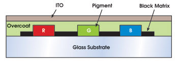
Figure 1. Part of the fabrication process for a color filter involves patterning its indium tin oxide (ITO) layer. The problem with using normally incident laser light to ablate the ITO is that the light is absorbed in the underlying black matrix, causing damage.
The solution has been to use a laser dry-etching process in which lasers precisely ablate material without chemicals. Although this has been successful in many applications, it has been less so in the ablation of ITO from color filters. The fundamental problem has been the differing absorption coefficients of the underlying materials and, especially, the high optical absorption of the black-matrix material, which is damaged easily by the optical power required to ablate the ITO.
ITO has a high absorption in the ultraviolet, so one possible solution would be to use deep-UV lasers to remove the material. Alternatively, the recent advent of ultrafast lasers has led to ultraprecise micromachining in many applications. However, when Naoaki Fukuda and his colleagues at Hitachi Zosen Corp. in Osaka, Japan, evaluated these techniques, they found that neither was suitable for patterning ITO on color filters.1
75° incidence
Instead, they developed an alternative process that they have shown to provide the required results. They used a Q-switched, diode-pumped solid-state laser to irradiate the ITO surface at an oblique angle — they found that a 75° angle was optimal — with 1-μm radiation. The oblique incidence meant that the light had to travel a greater distance through the ITO before reaching the black-matrix material, so more light was absorbed in the ITO. For the case of 75° incidence, the absorption was increased by 50 percent. This increased absorption was sufficient to etch the ITO without damaging the underlying black matrix.
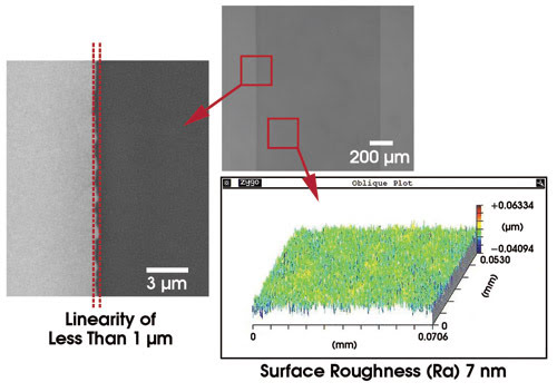
Figure 2. These experimental results from a scanning electron microscope (left) and a Zygo surface profiler (lower right) show that the grazing-incidence laser dry-etch process can be very useful not only in the fabrication of color filters but in other thin-film removal processes as well.
Figure 2 shows the results of the oblique-incidence laser dry etching. With a fluence of 0.5 J/cm2, Fukuda and his colleagues achieved a surface roughness (Ra) of 7 nm at the bottom of an etched groove, with no damage to the black matrix beneath. The linearity of the etch was better than 1 μm. Because the technique has been so successful at removing thin films in this demanding case, they believe that it also could find applications in many other specialized cases.
Flat panel displays that are based on organic light-emitting diodes (OLEDs) are very bright and colorful and exceptionally thin at the same time. They currently are mass-produced using a precision mask-patterning technique, but this technology cannot scale to larger sizes because of the unavoidable distortion of larger masks. Using white OLEDs and color filters has been investigated, but these methods have issues with power consumption and with color impurity. Another alternative is radiation-induced thermal transfer of organic material from a donor to a substrate, but until recently, this approach had been plagued with issues such as contact between the donor and the substrate, or mechanical and chemical instability of the donor.
Takashi Hirano and his colleagues at Sony’s Display Device Development Group in Atsugi, Japan, recently demonstrated a laser-induced thermal-transfer technique that avoids these issues.2 They used a rigid glass sample for the donor, avoiding the problem of mechanical and chemical instability, and separated the donor and substrate with pixel-defined spacers (Figure 3).
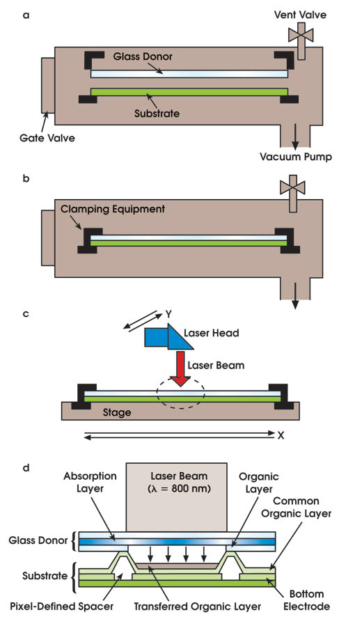
Figure 3. The glass donor and substrate are clamped together in a vacuum environment (a and b). The assembly then is illuminated with a scanning laser, which causes thermal transfer of organic material from the donor to the substrate (c). An enlargement of the circled area in 3c shows details of the transfer (d).
They placed the bottom electrode and the spacers onto the glass substrate and added organic common layers, such as the hole injection and hole transport layers. Meanwhile, they took a separate glass donor plate covered with a molybdenum absorption film and deposited organic material onto the molybdenum using a conventional evaporator.
Then they clamped together the donor and substrate in a vacuum environment so that atmospheric pressure would hold the two together when they were removed from the vacuum (Figure 3a and 3b). They placed the assembly — donor on top, substrate underneath — on a translation table beneath an 800-nm diode laser.
As the laser beam scanned a pattern on the surface of the donor, its energy was absorbed into the molybdenum, thermally transferring the same pattern of organic material to the substrate (Figures 3c and 3d).
They repeated the process with a different donor for each organic light-emission layer and finished the process by depositing common layers, such as the electron transport and the upper electrode, on top of the patterned organic layers. Because the laser-transfer process is performed at atmospheric pressure rather than in a vacuum, the entire fabrication cycle is simplified, and laser-positioning accuracy is enhanced.
Using this technique, Hirano and his colleagues fabricated a 27.3-in. active-matrix OLED display (Figure 4). In it, the blue-emitting layer is a common layer, and the red and green layers are deposited with the laser thermal-transfer technique described here. The display is quite vivid and only 10 mm thick. Its projected lifetime, however, is less than that of conventional OLED displays, but the Sony engineers are confident that further development efforts will remedy this shortcoming.
Microcrystalline silicon
The transistors in the backplane of the large display in Figure 4 also are the result of novel laser-based fabrication developed by Sony engineers. Historically, several technologies have been employed to fabricate the thin-film transistors (TFTs) that control the individual pixels of flat panel displays.
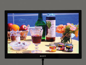
Figure 4. The 27.3-in. (diagonal) flat panel, active-matrix OLED display embodies both the laser transfer of organic materials and the laser annealing of thin-film transistors. ©Sony Corp.
These technologies have involved either crystalline or polycrystalline silicon as the semiconductor, but the subtleties of each technique have imposed limitations such as compensation circuits. Recently, attention has shifted to an approach employing microcrystalline silicon that seems to avoid or minimize these difficulties, and very recently Toshiaki Arai and his colleagues at Sony’s Display Device Development Group demonstrated a laser-based technique for fabricating these TFTs.3
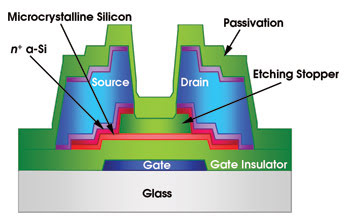
Figure 5. Sony engineers used a semiconductor laser to anneal the thin layer of amorphous silicon to form microcrystalline silicon between the source and the drain.
The new technique involves annealing a thin layer of silicon that connects the transistor’s source and drain (Figure 5). The external voltage applied to this layer controls the current that flows from the source to the drain, and typically these currents are high in an OLED display because OLEDs are high-current devices.
The transistor is fabricated by using standard lithography to deposit and pattern the various layers. The critical step here is thermally annealing the amorphous silicon layer (the pink layer in Figure 5) to form microcrystalline silicon. After depositing the amorphous silicon layer, the Sony engineers topped it with a thin molybdenum layer to provide the 800-nm absorption that is absent in amorphous silicon. They scanned it with 800-nm light from a laser diode array, whose energy is absorbed in the molybdenum and transferred to the silicon, which is annealed into the microcrystalline state (Figure 6). After crystallization, they etched off the molybdenum layer and deposited the additional layers shown in Figure 5.
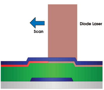
Figure 6. Absorbed by the molybdenum layer (blue) on top of the silicon (pink), the 800-nm laser radiation is converted to heat that anneals the amorphous silicon to its microcrystalline state.
Repair of broken conductors
Open-circuit defects among the thousands of individual conductors in a flat panel display are virtually impossible to avoid during manufacture. The problem becomes how to repair these defects quickly and inexpensively. Traditional remedies, such as laser chemical-vapor deposition and microdispenser methods, can make the repairs but can do so neither quickly nor inexpensively. One problem with these techniques is that the display usually must be removed from the assembly line for processing.
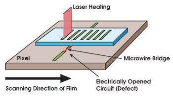
Figure 7. The pulsed laser radiation blasts a portion of the metal from the bottom of the glass donor substrate (light blue) onto the open-circuit defect beneath it.
Now, Eisaku Kojima and his colleagues at Omron in Kyoto, Japan, have developed a novel laser metal-transfer technique4 akin to the transfer technique for organic material described earlier in this article. A glass substrate coated with a metal film is positioned above the faulty conductor, and a pulsed laser beam is focused to the desired shape on the metal film. A portion of the metal, with the same shape as the laser beam, is transferred to the faulty conductor (Figure 7). The Omron engineers have used this technique successfully to repair open-circuit defects in conductors ranging from 1.5 to 7 μm in width. Using tantalum as the transfer material, they have obtained sheet resistance as small as 4.2 ohms per square. An analysis by energy-dispersive x-ray spectroscopy of the tantalum-aluminum boundary layer for the region indicated by the red arrow in Figure 8 has shown that a tantalum-aluminum alloy has been created by solid-phase diffusion, without heating the aluminum to its melting temperature.
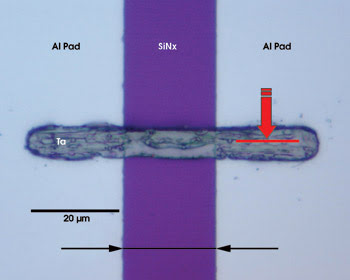
Figure 8. The transferred tantalum repairs the open-circuit defect between the two aluminum pads. Analysis of the region indicated by the red arrow has shown that the tantalum and aluminum form an alloy by solid-phase diffusion, without melting the aluminum.
Precision glass cutting
Microcracks or chipping defects in the edges of flat panel displays reduce the tensile strength of the entire glass sheet and diminish production yield and reliability of the display. Kimio Miyamoto and colleagues at LEMI in Osaka, Japan, recently demonstrated a laser glass-cutting technique that creates edges far superior to those made by conventional diamond scribing.5 Using a proprietary beam-shaping technology that they can fine-tune to obtain optimal results with various types of glasses, they scribe the cut with the laser’s focused output beam. The resulting edge quality is compared with an edge created with conventional diamond scribing in Figure 9. Because the laser scribing can trace an arbitrary pattern on the glass, free-form glass cutting is easily performed, as indicated in Figure 10.
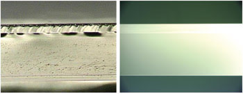
Figure 9. The glass cut with the precision laser technique (right) has a very smooth edge, free of microcracks and pitting defects that reduce the tensile strength of the entire glass sheet. For comparison, the photo on the left shows a glass edge cut by conventional diamond scribing. Courtesy of LEMI, Japan.
Meet the authors
Kunihiko Washio is president of Paradigm Laser Research, a consulting firm in Tokyo; e-mail: [email protected].
Breck Hitz is the senior technology editor of Photonics Spectra and executive director of LEOMA, the Laser and Electro-Optics Manufacturers’ Association; e-mail: [email protected].
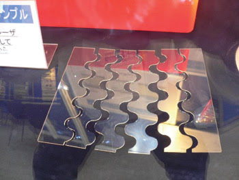
Figure 10. Free-form glass cutting is easy with the laser-scribing technique. Courtesy of LEMI of Osaka, Japan. The different forms (allotropes) of silicon.
References
1. N. Fukuda et al (2007). Dry-etching system with Q-switched DPSS laser for flat panel displays. Proc. LPM 2007-the 8th International Symposium on Laser Precision Microfabrication, #07-44: Th 4-06.
2. T. Hirano et al (2007). Novel laser transfer technology for manufacturing large-sized OLED displays. SID 07 Digest, p. 1592.
3. T. Arai et al (2007). Micro silicon technology for active matrix OLED display. SID 07 Digest, p. 1370.
4. E. Kojima and T. Wada (December 2007). Open mode defect repair for TFT LCD with laser metal transfer method. Proc. 67th Laser Processing Society Conference, Tokyo, p. 109 (in Japanese).
5. http://lemi.jp/tenji1.htm (in Japanese).
The different forms (allotropes) of silicon
Most semiconductor applications require crystalline silicon, in which all the atoms are arranged in a large, tetrahedral lattice. Crystalline silicon, as with YAG and many other commercial crystals, can be grown from the melt to a large-size boule by the Czochralski technique. Silicon also can exist in a disordered, amorphous form, in which the atoms are arranged randomly. Amorphous silicon usually is obtained by a deposition process as a film on a substrate.
Between these two allotropes of silicon, there are two other possibilities. Polycrystalline silicon (polysilicon) consists of many small grains of crystalline silicon, each typically tens or hundreds of nanometers in dimension. Microcrystalline silicon, sometimes called nanocrystalline silicon, is a mixture of very tiny crystalline grains — nanometers or tens of nanometers — and amorphous silicon. In microcrystalline silicon, at least 30 percent of the atoms are in the crystalline grains. Amorphous silicon can be transformed into microcrystalline or polycrystalline silicon by heat treatment such as laser annealing.