Excimer lasers are key to the low-temperature annealing of polycrystalline silicon for the volume production of flat panel displays. Manufacturers have responded to the needs of this application by developing a new generation of industrial excimer lasers that offer the necessary combination of high pulse energies and high energy stability.
Ludolf Herbst, Coherent GmbH
Many high-performance flat panel displays, including the latest active-matrix organic LED and system-on-panel devices, are based on polycrystalline silicon (“polysilicon”) rather than on the more widely used amorphous silicon. Low-temperature laser annealing is the preferred approach for producing the critical polysilicon layer during fabrication, with excimer laser annealing and sequential lateral solidification being the two established methods.
The various electronic components that comprise a flat panel display such as thin-film transistors, are patterned in a layer of silicon with a process analogous to that used for fabricating integrated circuits. The silicon layer is mass-produced by vapor deposition on a thin glass substrate. This yields amorphous silicon, which is suitable for some flat panel display applications, such as LCD televisions, but which is inappropriate for use in applications in which a long lifetime, high brightness, superior resolution and/or high frame rate are critical. These applications require polysilicon, which possesses an electron mobility that is orders of magnitude higher than amorphous silicon and better long-term reliability.
Amorphous silicon can be transformed into polysilicon by thermal annealing in a high-temperature oven, but this requires the use of expensive, heat-resistant varieties of glass, such as quartz, to avoid thermal stresses and the formation of microcracks. High-temperature polysilicon, therefore, is used only for special applications, such as LCD multimedia projectors.
Instead, all display products are based on low-temperature laser annealing using a 308-nm excimer laser. The 50- to 100-nm-thick film of amorphous silicon efficiently absorbs this wavelength at the surface, so it is rapidly heated to the melting point before significant heat diffusion to the rest of the glass can occur. This annealing process is performed at a temperature of only 200 °C, and it thus is compatible with standard, low-cost display glass.
Laser annealing
Excimer laser annealing, the first commercially successful low-temperature polysilicon annealing process, is used by a number of volume manufacturers of flat panel displays. In an excimer laser annealing system, the rectangular laser beam passes through homogenizing optics and is reshaped into a long, thin line. Using such a high-aspect-ratio beam shape enables the delivery of a high energy density, or fluence, at the panel to nearly completely melt the exposed silicon layer. This line shape also covers a large width, maximizing process speed and panel uniformity.
The homogeneity of the final beam is 2 percent (2 σ), which results in very consistent crystallization when the substrate is scanned with overlapping pulses. This line profile is directed at the silicon-coated substrate, which is translated perpendicularly to the beam. A complete system also incorporates alignment and automated-process monitoring tools, including a beam profiler and online pulse energy meters.
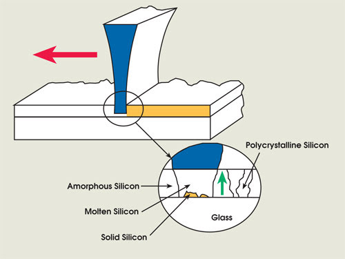
It is imperative that the amorphous silicon does not melt completely (Figure 1). A small residue of the unmelted material acts as a seed crystal that permits controlled growth upward from the interface with the melted silicon. Achieving this not quite complete melt requires tight control of the laser fluence.

Figure 1. In excimer laser annealing, the high-intensity line-shaped beam causes the nearly complete melt of the amorphous silicon layer. The liquid/solid interface seeds the crystallization process.
Several factors determine the delivered fluence, the most important of which being the pulse energy and the dimensions of the final line focus. A high pulse energy is critical to reaching the threshold for a nearly complete melt with a large line. A large line — chosen to match the width or half-width of a display panel — increases process throughput and results in a high depth of field, which in turn increases the process window, simplifying the system focus and further increasing the overall yield.
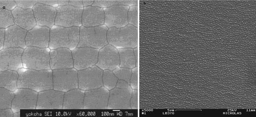
The latest excimer laser annealing systems offer pulse energies of more than 1 J and employ cylindrical optics to deliver line dimensions of 465 × 0.4 mm. With a typical pulse overlap of approximately 20 pulses per location, this delivers a crystallization speed of 28 cm2/s at a laser repetition rate of 300 Hz. The result is a homogeneous polysilicon film with a grain size of approximately 0.3 × 0.3 μm (Figures 2a and 2b), enabling N-channel electron mobility of 100 to 150 cm2/V·s.

Figure 2. Scanning electron micrographs reveal the structure of polysilicon created by excimer laser annealing at high (a) and low resolution (b). High-resolution micrograph courtesy of Japan Steel Works Ltd.
In contrast, sequential lateral solidification is designed to grow the crystal grains in a direction parallel to the display panel. It produces larger crystals than does excimer laser annealing. Because electron mobility scales with grain size, sequential lateral solidification yields higher-performance thin-film transistors, enabling the integration of driver circuits and system-on-glass technology.

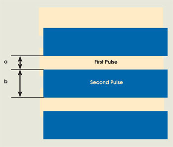
Figure 3. In the two-shot sequential lateral solidification process, the second pulse pattern (black) overlaps with the regions crystallized by first pulses (gray). This requires that the pattern space width “a” be smaller than the linewidth “b.”
Lateral crystal growth requires seeding from a vertical, solid silicon surface. This is done by using mask projection optics and a two-exposure process. The mask consists of a pattern of long stripes (Figure 3).
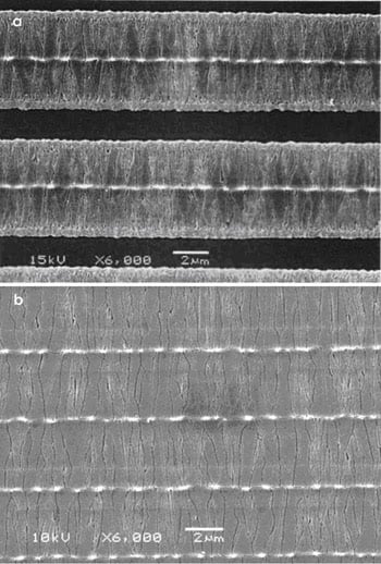
The first exposure produces a complete melt of the silicon layer in the exposed areas, resulting in alternating lines of polysilicon and amorphous silicon, with typical linewidths of a few microns (Figure 4a). The substrate then is translated, and a second exposure melts the previously unexposed areas. This yields a continuous layer of laterally crystallized polysilicon (Figure 4b). There is no limit on the panel size that can be processed in this manner.

Figure 4. Images of a 50-nm-thick layer of amorphous silicon show the crystallization after the first shot (a) and the final crystallization after the second (b). The beam edge of the second shot should overlap with the first. Courtesy of Japan Steel Works Ltd.
Besides the desirable grain characteristics, sequential lateral solidification has several practical advantages over excimer laser annealing. In particular, it has a higher throughput without added demands on the laser. Additionally, it offers a wider process window because the fluence must exceed the threshold for total melt rather than meet the narrow requirements for partial melt. It does require high-quality projection optics, however.
Laser performance
The low-temperature annealing of polysilicon has become a major application for excimer lasers. As they did with lasik and microlithography, manufacturers have responded by optimizing laser systems for the application. Because the requirements in this instance are particularly demanding, substantial improvements were necessary in virtually all areas of laser design and construction.
Low-temperature polysilicon currently is processed on fourth-generation substrates to produce panels as large as 720 × 930 mm, which then are split — or “singulated” — into a number of display units. The economical, high-throughput annealing of such large areas requires high laser powers.
For pulsed lasers, such high power can be accomplished by boosting the pulse energy or by increasing the repetition rate. In the past, industrial excimers were developed along two lines: high-pulse-energy lasers for such materials processing applications as ink-jet nozzle drilling, and high-repetition-rate lasers for such photolytic applications as lithography. Meeting the needs of excimer laser annealing and sequential lateral solidification requires both high pulse energies and high repetition rates.
High pulse energy enables a wider area to be processed with each pulse, while maintaining fluence levels in the process window. This, in turn, ensures a larger process window in terms of the depth of field and focusing parameters because the line must cover the entire panel width (or half the width in the latest generation of production lines) for process speed and panel uniformity. Conversely, low pulse energy would require an extremely thin line to reach the melting threshold, necessitating cylindrical optics with a high numerical aperture and, hence, a very shallow depth of field.
Before the advent of low-temperature polysilicon, high-energy excimer lasers had typical repetition rates of a few tens of hertz. This simply is too slow for the economical mass production of flat panel displays. As a result, the processing of this material has driven the development of specialized high-power excimer lasers that can deliver pulse energies in excess of 1 J while sustaining repetition rates of several hundred hertz.
Two other parameters of importance are the pulse-to-pulse stability and the laser’s reliability. Pulse-to-pulse stability translates directly into spatial uniformity of the annealing process and yield. It is particularly advantageous for high-performance active-matrix organic LED devices because it minimizes variation in the threshold voltage of the thin-film transistors, enabling their mass production. The use of novel active laser stabilization mechanisms enables the latest excimer lasers to deliver a 100 percent improvement in pulse-to-pulse variation: 0.5 percent rms, compared with 1 percent for earlier lasers.
Laser reliability is important because it directly affects the cost of ownership and overall process economics. The strong growth in industrial excimer applications has driven progress in the lifetime of all key components and consumables. But low-temperature polysilicon has put even greater demands on excimer technology. As the result of technical innovations such as all metal-ceramic laser tubes, long-lifetime optics and solid-state high-voltage switching, the lifetime for the tube in a 308-nm laser is now approximately 5 billion to 6 billion pulses versus 1 billion pulses 10 years ago.
Meet the author
Ludolf Herbst is product manager, industrial high-power excimer lasers, at Coherent GmbH in Göttingen, Germany; e-mail: [email protected].